ISD94100 Series Technical Reference Manual
Sep 9, 2019
Page
405
of 928
Rev1.09
IS
D
9
410
0
S
ER
IE
S
T
E
C
HN
ICA
L
RE
F
E
RE
NCE
M
AN
U
AL
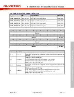
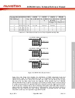
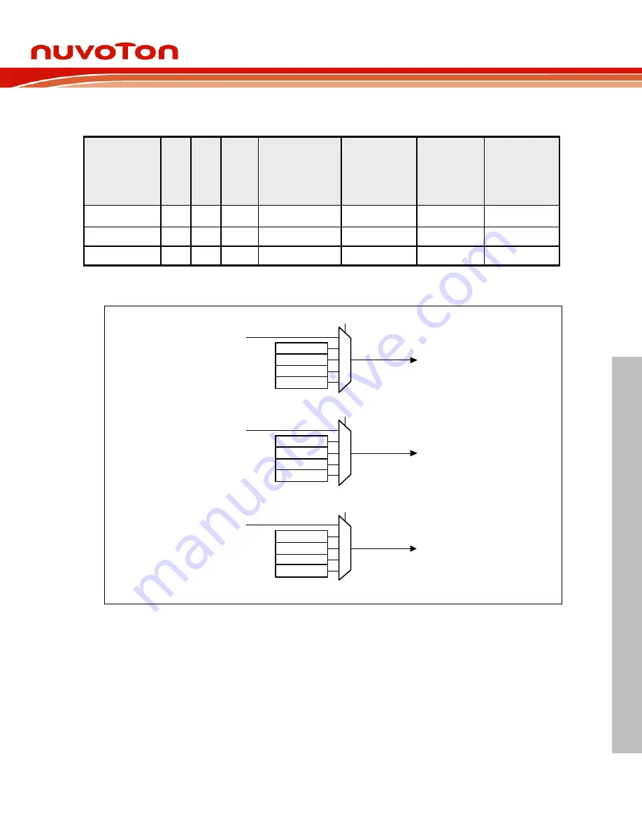
Table 6.8.3-1 PWM System Clock Source Control Registers Setting Table
PWM0 system clock
TIMER0
TIMER1
TIMER2
TIMER3
0
1
2
3
4
ECLKSRC0 (PWM0_CLKSRC[2:0])
PWM0_CLK0
PWM0 system clock
TIMER0
TIMER1
TIMER2
TIMER3
0
1
2
3
4
ECLKSRC2 (PWM0_CLKSRC[10:8])
PWM0_CLK2
PWM0 system clock
TIMER0
TIMER1
TIMER2
TIMER3
0
1
2
3
4
ECLKSRC4 (PWM0_CLKSRC[18:16])
PWM0_CLK4
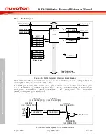
Figure 6.8-3 PWM Clock Source Control
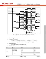
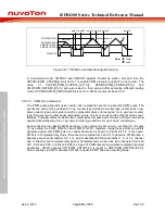
Figure 6.8-4 and Figure 6.8-5 illustrate the architecture of PWM independent mode and
complementary mode. No matter independent mode or complementary mode, paired channels’
(PWM_CH0 and PWM_CH1, PWM_CH2 and PWM_CH3, PWM_CH4 and PWM_CH5) counters
both come from the same clock source and prescaler. When counter count to 0, PERIOD
(PWM_PERIODn[15:0]) or equal to comparator, events will be generated. These events are passed
to corresponding generators to generate PWM pulse, interrupt signal and trigger signal for EADC
to start conversion. Output control is used to changing PWM pulse output state; brake function in
output control also generates interrupt events. In complementary mode, synchronize function is
available and even channel use odd channel comparator to generate events, free trigger
comparator events only use to generate trigger EADC signals.
Frequency Ratio
PCLK:PWM Clock
HCLK PCLK
PWM
Clock
HCLKSEL
CLK_CLKSEL0[2:0]
HCLKDIV
CLK_CLKDIV0[3:
0]
APBnDIV
(CLK_CLKDIVn
[2+4n:4n]),
N Denotes 0 Or
1
PWMnSEL
(CLK_CLKSEL2[N
]),
N Denotes 0 Or 1
1:1
HCLK PCLK
PCLK
Don’t care
Don’t care
Don’t care
1
1:2
PLL
PLL/ 2
PLL
2
0
1
0
1:2
PLL/ 2 PLL/ 2
PLL
2
1
0
0

