ISD94100 Series Technical Reference Manual
Sep 9, 2019
Page
433
of 928
Rev1.09
IS
D
9
410
0
S
ER
IE
S
T
E
C
HN
ICA
L
RE
F
E
RE
NCE
M
AN
U
AL
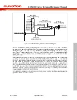
BRKEIF0 (PWM_INISTS1[0])
BRKEIF1 (PWM_INTSTS1[1])
BRK_INT
BRKEIEN0_1 (PWM_INTEN1[0])
CRLIF0 (PWM_CAPIF[0])
PWM_INT
CAP_INT
ZIEN0 (PWM_INTEN0[0])
ZIF0 (PWM_INTSTS0[0])
PIEN0 (PWM_INTEN0[8])
PIF0 (PWM_INTSTS0[8])
CMPUIEN0 (PWM_INTEN0[16])
CMPUIF0 (PWM_INTSTS0[16])
CMPDIEN0 (PWM_INTEN0[24])
CMPDIF0 (PWM_INTSTS0[24])
ZIEN1 (PWM_INTEN0[1])
ZIF1 (PWM_INTSTS0[1])
PIEN1 (PWM_INTEN0[9])
PIF1 (PWM_INTSTS0[9])
CMPUIEN1 (PWM_INTEN0[17])
CMPUIF1 (PWM_INTSTS0[17])
CMPDIEN1 (PWM_INTEN0[25])
CMPDIF1 (PWM_INTSTS0[25])
CAPRIEN0 (PWM_CAPIEN[0])
CFLIF0 (PWM_CAPIF[8])
CAPFIEN0 (PWM_CAPIEN[8])
CRLIF1 (PWM_CAPIF[1])
CAPRIEN1 (PWM_CAPIEN[1])
CFLIF1 (PWM_CAPIF9])
CAPFIEN1 (PWM_CAPIEN[9])
BRKLIF0 (PWM_INISTS1[8])
BRKLIF1 (PWM_INISTS1[9])
BRKLIEN0_1 (PWM_INTEN1[8])
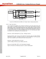
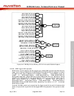
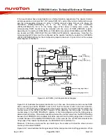
Figure 6.8-37 PWM0_CH0 and PWM0_CH1 Pair Interrupt Architecture Diagram
6.8.5.26 PWM Trigger EADC Generator
PWM can be one of the EADC conversion trigger source. Each PWM pair channels share the same
trigger source. Setting TRGSELn bit of PWM_ADCTS0 and PWM_ADCTS1 registers is to select
the trigger sources, where TRGSELn bit is TRGSEL0, TRGSEL1, …, and TRGSEL5, which are
located in PWM_EADCTS0[3:0], PWM_EADCTS0[11:8], PWM_EADCTS0[19:16],
PWM_EADCTS0[27:24], PWM_EADCTS1[3:0] and PWM_EADCTS1[11:8], respectively. Setting
TRGENn bit of PWM_EADCTS0 and PWM_EADCTS1 registers is to enable the trigger output to
EADC, where TRGENn bit is TRGEN0, TRGEN1, …, TRGEN5, which are located in
PWM_EADCTS0[7], PWM_EADCTS0[15], PWM_EADCTS0[23], PWM_EADCTS0[31],
PWM_EADCTS1[7] and PWM_EADCTS1[15], respectively. The number n (n = 0,1, ..,5) denotes
PWM channel number.
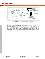
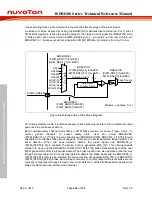
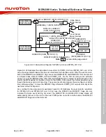
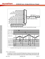
There are 16 PWM events can be selected as the trigger source for one pair of channels which
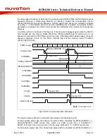
shown in Figure 6.8-38. Figure 6.8-39 is the trigger EADC timing waveform in the up-down counter
type.


