ISD94100 Series Technical Reference Manual
Sep 9, 2019
Page
589
of 928
Rev1.09
IS
D
9
410
0
S
ER
IE
S
T
E
C
HN
ICA
L
RE
F
E
RE
NCE
M
AN
U
AL
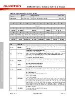
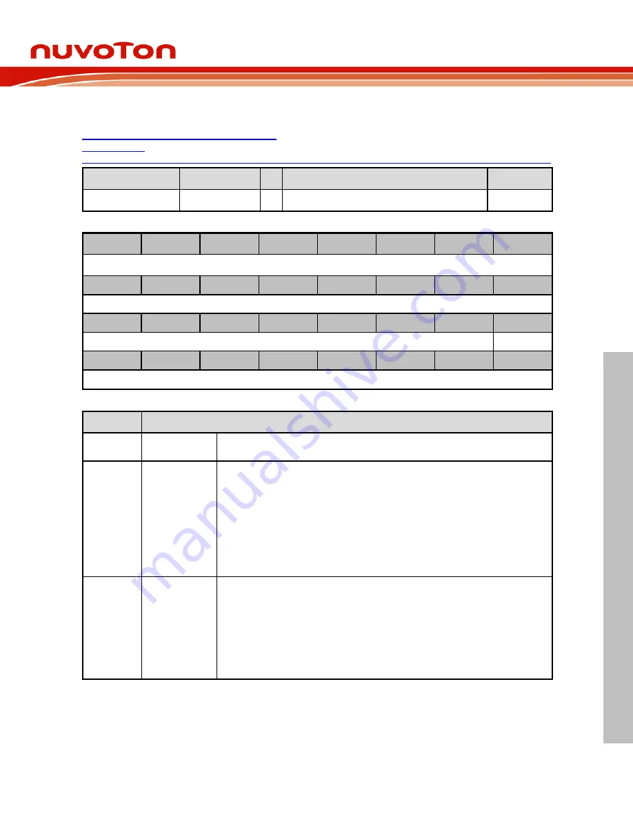
6.12.7 Register Description
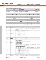
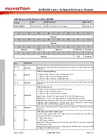
UART Receive/Transmit Buffer Register
(UART_DAT)
Register
Offset
R/W Description
Reset Value
UART_DAT
U0x00
R/W UART Receive/Transmit Buffer Register
0x0000_0000
31
30
29
28
27
26
25
24
Reserved
23
22
21
20
19
18
17
16
Reserved
15
14
13
12
11
10
9
8
Reserved
PARITY
7
6
5
4
3
2
1
0
DAT
Bits
Description
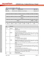
[31:9]
Reserved
Reserved. Any values read should be ignored. When writing to this field always write with
reset value.
[8]
PARITY
Parity Bit Receive/Transmit Buffer
Write Operation:
By writing to this bit, the parity bit will be stored in transmitter FIFO. If PBE (UART_LINE[3])
and PSS (UART_LINE[7]) are set, the UART controller will send out this bit follow the DAT
(UART_DAT[7:0]) through the UART0_TXD pin.
Read Operation:
If PBE (UART_LINE[3]) and PSS (UART_LINE[7]) are enabled, the parity bit can be read by
this bit.
Note:
This bit has effect only when PBE (UART_LINE[3]) and PSS (UART_LINE[7]) are set.
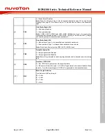
[7:0]
DAT
Data Receive/Transmit Buffer
Write Operation:
By writing one byte to this register, the data byte will be stored in transmitter FIFO. The
UART controller will send out the data stored in transmitter FIFO top location through the
UART0_TXD pin.
Read Operation:
By reading this register, the UART controller will return an 8-bit data received from receiver
FIFO.

