ISD94100 Series Technical Reference Manual
Sep 9, 2019
Page
696
of 928
Rev1.09
IS
D
9
410
0
S
ER
IE
S
T
E
C
HN
ICA
L
RE
F
E
RE
NCE
M
AN
U
AL
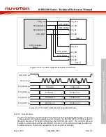
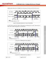
Figure 6.14-25 TX Underflow Event and Slave Under Run Event
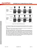
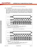
In 2-Bit Transfer mode, the transmit data is loaded into shift register after 2 datum have been written
into the TX FIFO buffer. It uses two shift registers and two 4-level skew buffers concurrently. The
detail timing of 2-Bit Transfer mode, please refer to the section of Two-Bit Transfer mode.
TXEMPTY = 1
Data 0
TXEMPTY = 0
Write
2 Data
TXEMPTY = 1
H/W load TX
Buffer into
Shift Register
b31|b30...b1|b0
TXEMPTY = 1
Data0
0 0 b31...b4|b3
Data0
b0
b1
b2
TX Buffer
TX Shift Register
TX Skew Buffer
H/W load Shift
Register into
Skew Buffer
Data 1
b31|b30...b1|b0
Data1
b0
b1
b2
0 0 b31...b4|b3
Data1
SPI0_MOSI0
SPI0_MOSI1
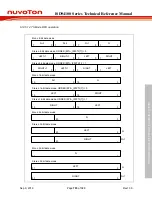
Example :
SPI0
TWOBIT = 1
DWIDTH =0
LSB = 1
Figure 6.14-26 Two-Bit Transfer Mode FIFO Buffer Example (SPI0 Only)
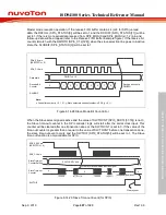
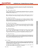
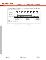
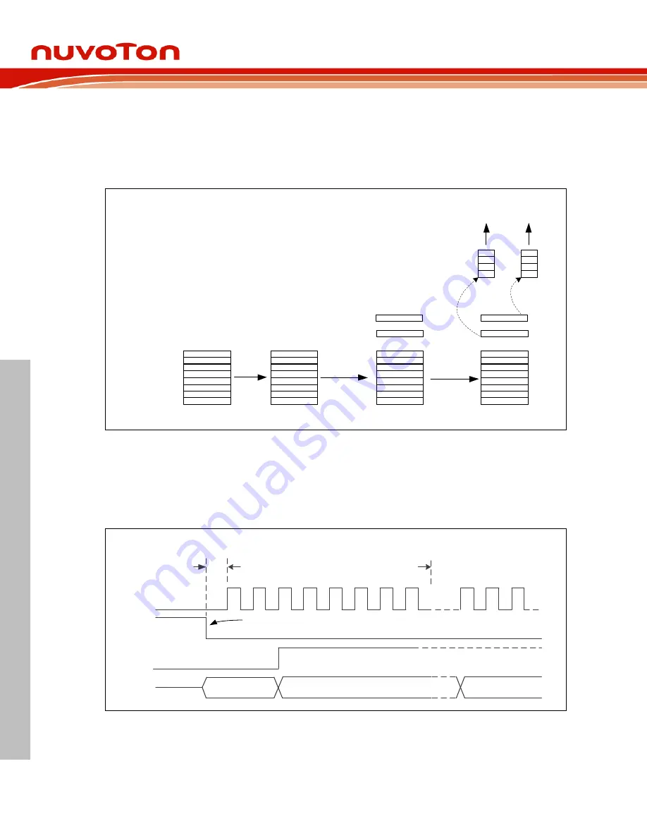
In SPI0 Slave 3-Wire mode, the first 2-bit data is un-predicted (keep on the level of last bit in
previously transfer) if the data is written into TX FIFO among 3 peripheral clock cycles before the
SPI bus clock is presented. The other bits are held by TXUFPOL (SPI0_FIFOCTL[6]) because there
is TX underflow event. The written data will be transmitted in the next transfer.
SPI0_CLK
SPI0_MISO0
TXEMPTY
TXUFPOL
TXUFIF
Data 0 is written into TX FIFO Buffer among 3 peripheral
clock cycles before SPI bus clock is presented
Data 0
Unknown
1st transaction word
Less than 3 slave
peripheral clock cycles
Figure 6.14-27 TX Underflow Event (SPI0 Slave 3-Wire Mode Enabled)
In Slave mode, during receiving operation, the serial data is received from SPI0_MOSI0 and
SPIx_MOSI (x=1, 2) pin and stored to SPIn_RX register. The reception mechanism is similar to


