ISD94100 Series Technical Reference Manual
Sep 9, 2019
Page
869
of 928
Rev1.09
IS
D
9
410
0
S
ER
IE
S
T
E
C
HN
ICA
L
RE
F
E
RE
NCE
M
AN
U
AL
Digital MIC
SEL
CLK
DAT
Digital MIC
SEL
CLK
DAT
DMIC_DATn
DMIC_CLKn
Note:
n = 0 or 1
VDD
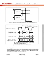
Figure 6.19-3 Typical connection to two digital microphones sharing a common data line
MIC0
Data
MIC0
Data
MIC1
Data
MIC1
Data
MIC0
Data
MIC1
Data
MIC0
Data
MIC1
Data
DMIC Bus Clock on DMIC_CLK0 pin
Digital MIC0 PDM data output
Digital MIC1 PDM data output
PDM data on DMIC_DAT0 pin
(Digital MIC0/1 output interleaved)
High Z
High Z
High Z
High Z
Note:
MIC0 PDM data for DMIC channel 0 and MIC1 PDM data for DMIC
channel 1 when LCHEDGE01 (DMIC_CTL[8]) = 0
Latched PDM Data on Falling Clock Edge
Latched PDM Data on Rising Clock Edge
Figure 6.19-4 Digital Microphone Interface Timing Diagram
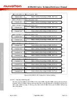
6.19.5.5 FIFO Operation
FIFO bits is 24 bits. ISD94100 series supports four channel digital microphone inputs, each channel
can be enabled by register CHENn (DMIC_CTL[3:0]) (n = 0, 1, 2 and 3). The memory arrangements
of PCM data for various settings are shown in Figure 6.19-5.

