ISD94100 Series Technical Reference Manual
Sep 9, 2019
Page
871
of 928
Rev1.09
IS
D
9
410
0
S
ER
IE
S
T
E
C
HN
ICA
L
RE
F
E
RE
NCE
M
AN
U
AL
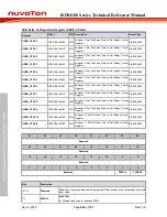
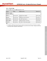
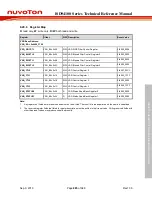
6.19.6 Register Map
R
: read only,
W
: write only,
R/W
: both read and write.
Register
Offset
R/W Description
Reset Value
DMIC Base Address:
DMIC_BA = 0x4006_3000
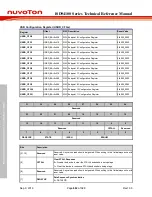
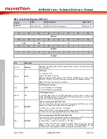
DMIC_CTL
0x00
R/W DMIC Control Register
0xB7CD_0000
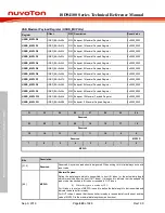
DMIC_DIV
0x04
R/W DMIC Clock Divider Register
0x0000_0307
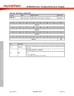
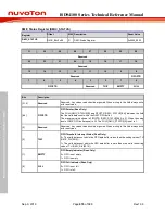
DMIC_STATUS
0x08
R
DMIC Status Register
0x0000_0002
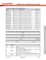
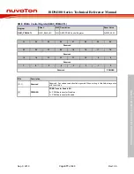
DMIC_PDMACTL
0x0C
R/W DMIC PDMA Control Register
0x0000_0000
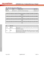
DMIC_FIFO
0x10
W
DMIC FIFO Data Output Register
0x0000_0000
Note:
1.
Any register not listed here is reserved and must not be written. The result of a read operation on these bits is undefined.
2.
The reserved register fields that listed in register description must be written to their reset value. Writing reserved fields with
other than reset values may produce undefined results.


