ISD94100 Series Technical Reference Manual
Sep 9, 2019
Page
886
of 928
Rev1.09
IS
D
9
410
0
S
ER
IE
S
T
E
C
HN
ICA
L
RE
F
E
RE
NCE
M
AN
U
AL
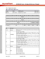
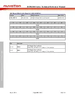
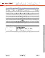
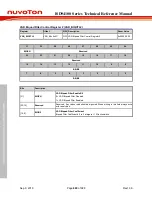
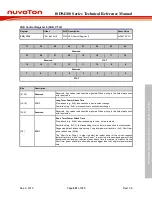
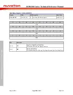
6.20.7 Register Description
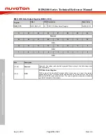
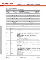
VAD SINC Filter Control Register (VAD_SINCCTL)
Register
Offset
R/W Description
Reset Value
VAD_SINCCTL
0x00
R/W VAD SINC Filter Control Register
0x0000_0008
31
30
29
28
27
26
25
24
VADEN
ACTCL
SW
DATAOFF
Reserved
23
22
21
20
19
18
17
16
Reserved
15
14
13
12
11
10
9
8
Reserved
SINCOSR
7
6
5
4
3
2
1
0
Reserved
Bits
Description
[31]
VADEN
VAD Enable Control
0 = VAD Disabled.
1 = VAD Enabled.
Note 1:
When set this bit to 1, CHEN0 (DMIC_CTL[0]) will be set to 1 and CHEN1
(DMIC_CTL[1]), CHEN2 (DMIC_CTL[2]) and CHEN3 (DMIC_CTL[3]) will be set to 0
automatically.
Note 2:
When set this bit to 1, DMIC_CLK is generated by VAD module.
[30]
ACTCL
VAD Active Flag Clear
0 = No effect.
1 = Clear ACTIVE(VAD_STATUS0[31]).
Note:
After ACTIVE(VAD_STATUS0[31]) is cleared, user need to set set this bit to 0.
[29]
SW
VAD Path Switch Control
After the ACTIVE(VAD_STATUS0[31]) goes high, it will automatically switch to the
DMIC path. When the CPU is entering idle mode, write 1 to switch back to the VAD path.
Note 1:
After switch back VAD path, user need to set this bit to 0.
Note 2:
User need to set DMIC_CTL[3:0] to 1 and clear ACTIVE (VAD_STATUS0[31])
before set this bit 1.
[28]
DATAOFF
VAD Sending Data to SRAM Control
When the ACTIVE (VAD_STATUS0[31]) goes high, the data will be transferred to SRAM
to store which can be used for keyword detection later. After some time, if user needs
to stop sending data to SRAM, write this bit to 1.
[27:12]
Reserved
Reserved. Any values read should be ignored. When writing to this field always write
with reset value.
[11:8]
SINCOSR
VAD SINC Filter OSR Setting
000 = Down sample 48
001 = Down sample 64

