ISD94100 Series Technical Reference Manual
Sep 9, 2019
Page
167
of 928
Rev1.09
IS
D
9
410
0
S
ER
IE
S
T
E
C
HN
ICA
L
RE
F
E
RE
NCE
M
AN
U
AL
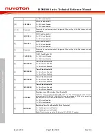
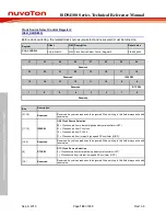
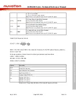
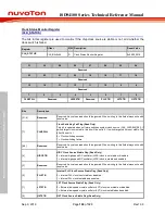
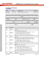
0 = PLL is in normal mode.
1 = PLL is in Power-down mode (default).
Note:
This bit is write protected. Refer to the SYS_REGLCTL register.
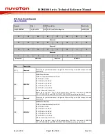
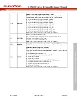
[15:14]
OUTDIV
PLL Output Divider Control (Write Protected)
Refer to the formulas below the table.
Note:
This bit is write protected. Refer to the SYS_REGLCTL register.
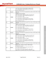
[13:9]
INDIV
PLL Input Divider Control (Write Protected)
Refer to the formulas below the table.
Note:
This bit is write protected. Refer to the SYS_REGLCTL register.
[8:0]
FBDIV
PLL Feedback Divider Control (Write Protected)
Refer to the formulas below the table.
Note:
This bit is write protected. Refer to the SYS_REGLCTL register.
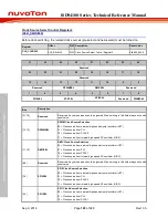
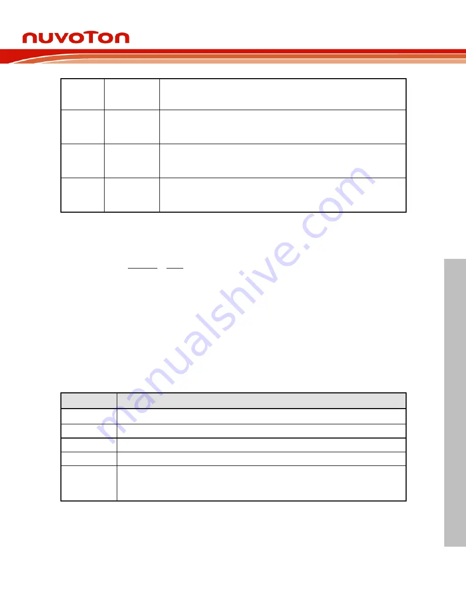
Output Clock Frequency formula:
NO
NR
NF
FIN
FOUT
1
*
2
×
×
=
FREF = FIN / NR, where FREF is the comparison frequency for the PFD (phase frequency detector).
FVCO = FOUT * NO
For proper operation in normal mode, the following constraints must be satisfied:
4 MHz ≤ FREF ≤ 8 MHz
200 MHz ≤ FVCO ≤ 500 MHz
50 MHz ≤ FOUT ≤
200 MHz
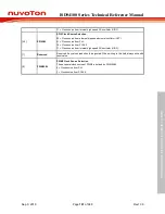
Symbol
Description
FOUT
Output Clock Frequency
FIN
Input (Reference) Clock Frequency
NR
Input Divider (INDIV + 1)
NF
Feedback Divider (FBDIV + 2)
NO
OUTDIV = “00” : NO = 1
OUTDIV = “01” : NO = 2
OUTDIV = “10” : NO = 2
OUTDIV = “11” : NO = 4
Table 6.3.9-1 The symbol definition of PLL Output Frequency formula


