ISD94100 Series Technical Reference Manual
Sep 9, 2019
Page
192
of 928
Rev1.09
IS
D
9
410
0
S
ER
IE
S
T
E
C
HN
ICA
L
RE
F
E
RE
NCE
M
AN
U
AL
6.4.3
Block Diagram
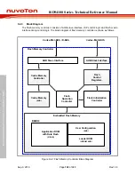
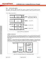
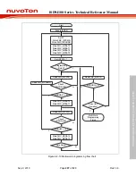
The flash memory controller consists of AHB slave interface, ISP control logic and flash macro
interface timing control logic. The block diagram of flash memory controller is shown as follows.
Flash
Operation
Controller
Flash Initialization
Controller
AHB Slave Interface
Embedded Flash Memory
Flash
Control
Registers
Cache Memory
Controller
AHB Slave Interface
Cortex-M4 S-BUS
Cortex-M4 I-BUS / D-BUS
Flash Memory Controller
Cache Memory
(4KB)
Application ROM
with Data Flash
(512KB)
User Configuration
(4KB)
Loader ROM
(LDROM 4KB)
BANK0
Figure 6.4-1 Flash Memory Controller Block Diagram


