ISD94100 Series Technical Reference Manual
Sep 9, 2019
Page
194
of 928
Rev1.09
IS
D
9
410
0
S
ER
IE
S
T
E
C
HN
ICA
L
RE
F
E
RE
NCE
M
AN
U
AL
6.4.4
Functional Description
This section describes ISD94100 series flash memory controller’s functions including memory
organization, boot configuration, IAP, ISP, Flash read/write operation, checksum calculation, and so on.
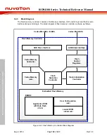
6.4.4.1 Memory Organization
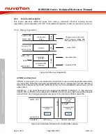
0x0000_0000
0x0007_FFFF
512
KB
ApplicationROM
(APROM)
Data Flash
(4*N)KB
DFBA
0x0010_0000
0x0010_FFFF
LDROM
0x0030_0000
0x0030_000B
Configuration
Bytes
4
KB
12
B
yte
Configure: security lock, boot
select, brown-out voltage, data
flash base address(DFBA), etc.
Loader ROM
Application ROM
Application data
Figure 6.4-2 Memory Organization
APROM and Data Flash
APROM is main memory for user applications. Data Flash is used to store application parameters
(not instruction). Data Flash is shared with APROM and size is configurable. The base address of
Data Flash is determined by DFBA (CONFIG1[19:0]). All of the embedded Flash memory is 4 KB
page erased.
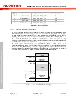
If DFEN bit = 1, the whole flash size will be assigned as APROM; if DFEN bit = 0, then area from
0x0000_0000 to DFBA-1 will be assigned to APROM, and the remaining flash size will be assigned
as Data Flash. See Configuration Bytes description for the definition of DFEN and DFBA.
0x0000_0000
APROM only
0x0007_FFFF
512
KB
ApplicationROM
(APROM)
ApplicationROM
(APROM)
APROM + Data flash
Data Flash
(4*N)KB
DFBA
vs.
DFEN=1
DFEN=0
EXAMPLE:
Figure 6.4-3 Data Flash Shared with 512 KB APRM example


