ISD94100 Series Technical Reference Manual
Sep 9, 2019
Page
52
of 928
Rev1.09
IS
D
9
410
0
S
ER
IE
S
T
E
C
HN
ICA
L
RE
F
E
RE
NCE
M
AN
U
AL
6.2.2.2 Power-on Reset (POR)
System power-on generates the Power-on reset (POR). When power is applied, the POR module
detects the rising voltage and generates reset signal. The reset signal stays active until the voltage
is ready for MCU operation. PORF bit (SYS_RSTSTS[0]) will be set to 1 to indicate a POR reset
event. The PORF bit (SYS_RSTSTS[0]) can be cleared by writing 1 to it.
6.2.2.3 Low Voltage Reset (LVR)
Writing 1 to LVREN bit (SYS_BODCTL[7]) enables the Low Voltage Reset (LVR) function. If enabled,
the LVR function module keeps monitoring V
DD
during system operation.
If V
DD
voltage has been lower than V
LVR
, a LVR reset will be triggered and the chip will be reset.
Once triggered, the LVR reset keeps the chip in reset state until the V
DD
voltage rises back and has
been above V
LVR
.
By default, Low Voltage Reset is enabled without De-glitch function.
6.2.2.4 Brown-out Detector Reset (BOD Reset)
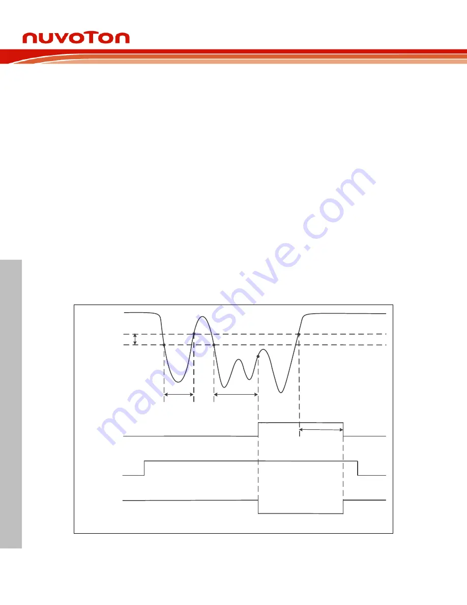
Writing 1 to Brown-out Detector Enable Bit BODEN (SYS_BODCTL[0]) enables the Brown-out
Detector (BOD) function. In addition, writing 1 to the BODRSTEN (SYS_BODCTL[3]) enables the
BOD reset function. When enabled, the BOD module monitors V
DD
during system operation, if V
DD
voltage is lower than V
BOD
(defined by BODVL bits in SYS_BODCTL[18:16]) for more than De-glitch
time (defined by BODDGSEL bits in SYS_BODCTL[10:8]), a BOD reset will be triggered. The BOD
reset keeps the chip in reset state until a condition is met that V
DD
voltage has been higher than
V
BOD
for more than De-glitch time (defined by BODDGSEL).
Initial values of BODEN, BODVL and BODRSTEN (SYS_BODCTL[3]) are defined in flash
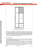
configuration byte CONFIG0. Figure 6.2-3 shows the Brown-out Detector waveform.
V
DD
V
BODL
BODOUT
BODRSTEN
Brown-out
Reset
T
1
(< BODDGSEL)
T
2
(= BODDGSEL)
T
3
(= BODDGSEL)
Hysteresis
V
BODH
Figure 6.2-3 Brown-out Detector (BOD) Waveform

