ISD94100 Series Technical Reference Manual
Sep 9, 2019
Page
530
of 928
Rev1.09
IS
D
9
410
0
S
ER
IE
S
T
E
C
HN
ICA
L
RE
F
E
RE
NCE
M
AN
U
AL
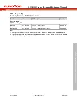
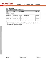
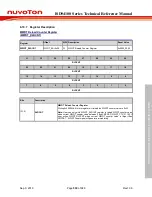
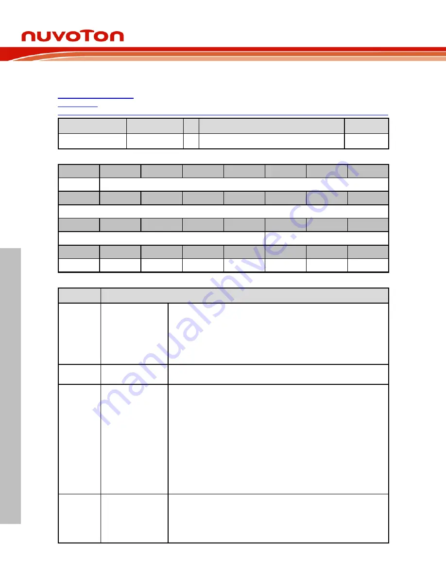
6.9.7
Register Description
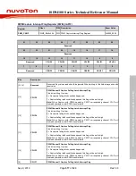
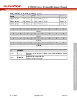
WDT Control Register
(WDT_CTL)
Register
Offset
R/W Description
Reset Value
WDT_CTL
0x00
R/W WDT Control Register
0x0000_07X0
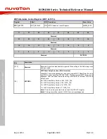
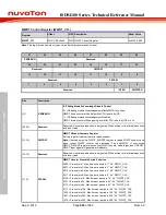
31
30
29
28
27
26
25
24
ICEDEBUG
Reserved
23
22
21
20
19
18
17
16
Reserved
15
14
13
12
11
10
9
8
Reserved
TOUTSEL
7
6
5
4
3
2
1
0
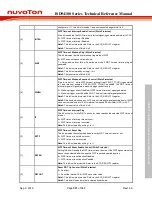
WDTEN
INTEN
WKF
WKEN
IF
RSTF
RSTEN
RSTCNT
Bits
Description
[31]
ICEDEBUG
ICE Debug Mode Acknowledge Disable Control (Write Protected)
0 = ICE debug mode acknowledgement affects WDT counting.
WDT up counter will be held while CPU is held by ICE.
1 = ICE debug mode acknowledgement Disabled.
WDT up counter will keep going no matter CPU is held by ICE or not.
Note:
This bit is write protected. Refer to the SYS_REGLCTL register.
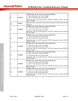
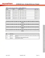
[30:11]
Reserved
Reserved. Any values read should be ignored. When writing to this field always write
with reset value.
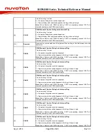
[10:8]
TOUTSEL
WDT Time-out Interval Selection (Write Protected)
These three bits select the time-out interval period for the WDT.
000 = 2
4
* WDT_CLK.
001 = 2
6
* WDT_CLK.
010 = 2
8
* WDT_CLK.
011 = 2
10
* WDT_CLK.
100 = 2
12
* WDT_CLK.
101 = 2
14
* WDT_CLK.
110 = 2
16
* WDT_CLK.
111 = 2
18
* WDT_CLK.
Note:
This bit is write protected. Refer to the SYS_REGLCTL register.
[7]
WDTEN
WDT Enable Control (Write Protected)
0 = WDT Disabled (This action will reset the internal up counter value).
1 = WDT Enabled.
Note1:
This bit is write protected. Refer to the SYS_REGLCTL register.
Note2:
If CWDTEN[2:0] (combined by Config0[31] and Config0[4:3]) bits is not

