ISD94100 Series Technical Reference Manual
Sep 9, 2019
Page
63
of 928
Rev1.09
IS
D
9
410
0
S
ER
IE
S
T
E
C
HN
ICA
L
RE
F
E
RE
NCE
M
AN
U
AL
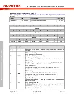
System Controllers Space (0xE000_E000 ~ 0xE000_EFFF)
0xE000_E010 – 0xE000_E0FF
SCS_BA
System Timer Control Registers
0xE000_E100 – 0xE000_ECFF
SCS_BA
External Interrupt Controller Control Registers
0xE000_ED00 – 0xE000_ED8F
SCS_BA
System Control Registers
Table 6.2.7-1 Address Space Assignments for On-Chip Controllers
6.2.8
SRAM Memory Organization
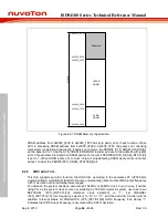
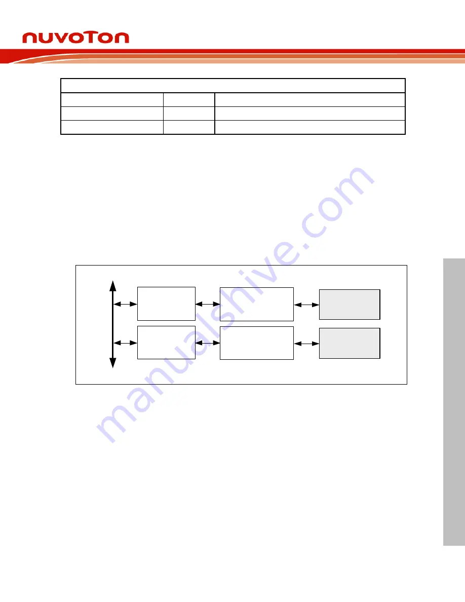
The ISD94100 series supports up to 192 KB of embedded SRAM and the SRAM organization is
separated to two banks: SRAM bank0 and SRAM bank1. The SRAM bank0 supports parity error
check to make sure chip operating more stable.
Supports up to 192 KB of SRAM
Supports byte / half word / word write
Supports parity error check function for SRAM bank0
Supports oversize response error
SRAM bank1
SRAM decoder
AHB interface
controller
SRAM bank0
SRAM decoder
AHB interface
controller
Figure 6.2-6 SRAM Block Diagram

