ISD94100 Series Technical Reference Manual
Sep 9, 2019
Page
765
of 928
Rev1.09
IS
D
9
410
0
S
ER
IE
S
T
E
C
HN
ICA
L
RE
F
E
RE
NCE
M
AN
U
AL
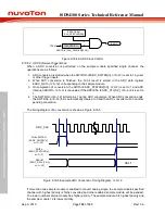
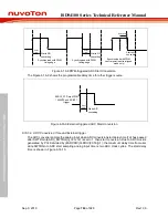
Idle state
Sampling
Hold
1 ADC clock
A/D conversion time
ADIFn
(EADC_STATUS2[n],
n=0~3)
ADC Status
ADC start
SWTRGn
(EADC_SWTRG
[n],
n=0~12)
PWRITE
PCLK
End of conversion
First ADC clock
Synchronous to
ADC clock delay
up to 1 ADC clock
A/D conversion start
delay time (Td)
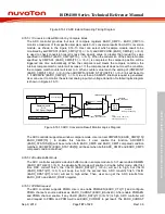
Figure 6.16-10 Conversion Start Delay Timing Diagram
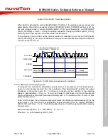
ADC conversion can be triggered by external pin EADC0_ST request. Setting the TRGSEL
(EADC_SCTLn[20:16], n=0~12) to 0x01 is to select external trigger input from the EADC0_ST pin.
User can set EXTFEN (EADC_SCTLn[5], n=0~12) and EXTREN (EADC_SCTLn[4], n=0~12) to
enable pin EADC0_ST trigger condition is falling or rising edge. There is a de-bounce circuit to
detect falling or rising edge. If rising edge trigger condition is selected, the low state must be kept
at least 2 PCLK cycles and the following high state must be kept at least 3 PCLK cycles. If falling
edge trigger condition is selected, the high state must be kept at least 2 PCLK cycles and the
following low state must be kept at least 3 PCLK cycles. Pulse that is shorter than this specification
will be ignored. The external trigger timing is shown in Figure 6.16-11

