ISD94100 Series Technical Reference Manual
Sep 9, 2019
Page
868
of 928
Rev1.09
IS
D
9
410
0
S
ER
IE
S
T
E
C
HN
ICA
L
RE
F
E
RE
NCE
M
AN
U
AL
DMIC_MCLK.
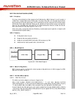
6.19.5.3 Determine DMIC Bus Clock and DMIC Working Main Clock
Determine DMIC working main clock (DMIC_MCLK) by:
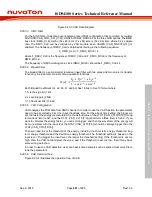
F_DMIC_MCLK = Fs * K;
K must be 500 or 256.
Where Fs is sample rate, and F_DMIC_MCLK is the frequency of DMIC_MCLK.
Determine DMIC bus clock (DMIC_CLK) by:
F_DMIC_CLK = Fs * OSR.
Where F_DMIC_CLK is the frequency of DMIC_CLK, and OSR is over sampling rate that is
controlled by register OSR (DMIC_CTL[6:4]). The example for DMIC clock and OSR configuring is
shown in Table 6.19.5-1.
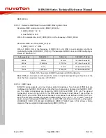
Fs (Sample Rate)
DMIC_MCLK
DMIC_CLK
OSR (DMIC_CTL[6:4])
48 KHz
24 MHz
2.4 MHz
100 (Down Sample 50)
48 KHz
12.288MHz
3.072 MHz
001 (Down Sample 64)
16 KHz
8 MHz
1.6 MHz
100 (Down Sample 100)
16 KHz
4.096 MHz
2.048 MHz
010 (Down Sample 128)
Table 6.19.5-1 Example for DMIC bus clock and OSR configuring
Note:
DMIC_CLK outputs select between the stereo microphones depending on the phase of the
clock that has a maximum frequency of 3.25 MHz.
6.19.5.4 DMIC Inputs
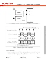
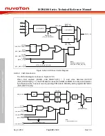
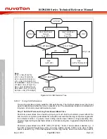
ISD94100 series supports up to four channel digital microphones. Two channel of PDM data are
multiplexed on the DMIC_DAT0 pin and the other two channel are multiplexed on the DMIC_DAT1
pin. The digital microphones are clocked by DMIC_CLK0 and DMIC_CLK1 pin. The general
connection is shown in Figure 6.19-3. The PDM data of channel 0 and channel 1 are latched on
DMIC_DAT0 pin, and the PDM data of channel 2 and channel 3 are latched on DMC_DAT1 pin.
Each channel can be enabled by register CHENn (DMIC_CTL[3:0]) (n = 0, 1, 2 and 3). User can
decide rising or falling edge of DMIC bus clock to latch PDM data for each channel by using register
LCHEDGE01 (DMIC_CTL[8]) and LCHEDGE23 (DMIC_CTL[9]). Figure 6.19-4 shows a timing
diagram of the two digital microphones sharing DMIC_DAT0 pin.


