ISD94100 Series Technical Reference Manual
Sep 9, 2019
Page
910
of 928
Rev1.09
IS
D
9
410
0
S
ER
IE
S
T
E
C
HN
ICA
L
RE
F
E
RE
NCE
M
AN
U
AL
6.21.7 Register Description
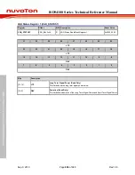
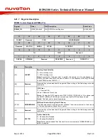
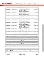
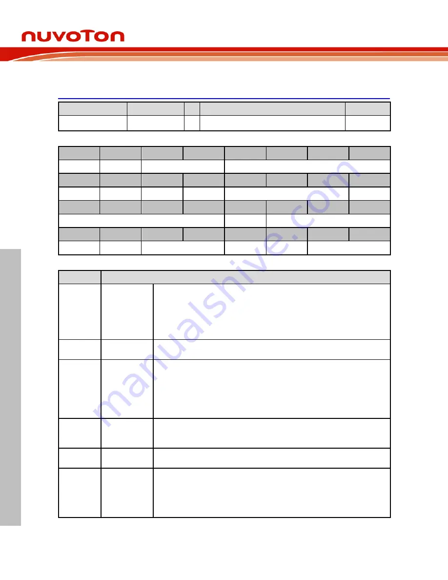
DPWM Control Register (DPWM_CTL)
Register
Offset
R/W Description
Reset Value
DPWM_CTL
0x00
R/W DPWM Control Register
0x0000_0600
31
30
29
28
27
26
25
24
CLKSET
Reserved
FCLR
BIQBANDNUM
23
22
21
20
19
18
17
16
Reserved
SPLTON
BIQON
FLTEN
FLTINTBIT
TH
15
14
13
12
11
10
9
8
TH
THIE
Reserved
7
6
5
4
3
2
1
0
DRVEN
DPWMEN
Reserved
DEADTIME
Reserved
FIFOWIDTH
Bits
Description
[31]
CLKSET
Working Clock Selection
0 = 512 fs working clock
1 = 500 fs working clock
Note:
For example, if the user want to get 48 kHz sample rate (fs), the frequency of
DPWM_CLK need to be 24576 kHz when CLKSET = 0, the frequency of DPWM_CLK need
to be 24000 kHz when CLKSET = 1.
[30]
Reserved
Reserved. Any values read should be ignored. When writing to this field always write with
reset value.
[29:28]
FCLR
FIFO Clear
11 = Clear the FIFO.
Others = Reserved. Do not use.
Note 1:
To clear the FIFO, need to write FCLR (DPWM_CTL[29:28]) to 11b, and can read
the EMPTY (DPWM_STATUS[1]) bit to make sure that the FIFO has been cleared.
Note 2:
This field is auto cleared by hardware.
[27:24]
BIQBANDNUM
BIQ Band Number Setting (Total 10 Bands)
This field represents the required number of bands. The minimum number is 1 and can up
to 10 when user enables biquad filter or splitter.
[23]
Reserved
Reserved. Any values read should be ignored. When writing to this field always write with
reset value.
[22]
SPLTON
Splitter Enable Bit
0 = 4-band splitter Disabled.
1 = 4-band splitter Enabled.
Note:
Splitter shared biquad filter 4 bands, the minimum number of BIQBANDNUM is 4, if
splitter is enabled.

