Nvis 5586A
Nvis Technologies Pvt. Ltd.
19
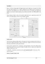
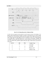
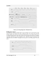
Read Cycle Timing Diagram for Minimum Mode
A write cycle also begins with the assertion of ALE and the emission of the address. The
M/IO* signal is again asserted to indicate a memory or I/O operation. In T2, after sending
the address in T1, the processor sends the data to be written to the addressed location. The
data remains on the bus until middle of T4 state. The WR* becomes active at the beginning
of T2 (unlike RD* is somewhat delayed in T2 to provide time for floating). The BHE and
A0 signals are used to select the proper byte or bytes of memory or I/O word to be read or
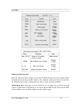
write. The M/IO*, RD* and WR* signals indicate the type of data transfer as specified in
table below.
Summary of Contents for 5586A
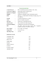
Page 2: ...Nvis 5586A Nvis Technologies Pvt Ltd 2...
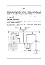
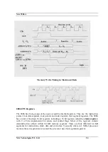
Page 23: ...Nvis 5586A Nvis Technologies Pvt Ltd 23 Memory Read Timing in Maximum Mode...
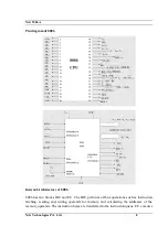
Page 30: ...Nvis 5586A Nvis Technologies Pvt Ltd 30...
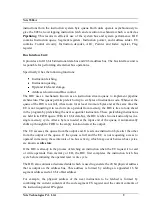
Page 48: ...Nvis 5586A Nvis Technologies Pvt Ltd 48 Diagram of module RESET power Instruction Set Note...

