Nvis 5586A
Nvis Technologies Pvt. Ltd.
21
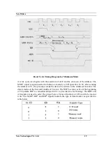
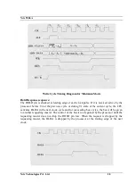
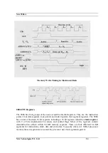
Bus Request and Bus Grant Timings in Minimum Mode System
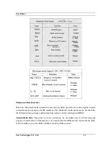
Maximum Mode 8086 System
In the maximum mode, the 8086 is operated by strapping the MN/MX* pin to ground. In this
mode, the processor derives the status signal S2*, S1*, S0*. Another chip called bus
controller derives the control signal using this status information. In the maximum mode,
there may be more than one microprocessor in the system configuration. The components in
the system are same as in the minimum mode system. The basic function of the bus
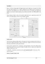
controller chip IC8288, is to derive control signals like RD* and WR* (for memory and I/O
devices), DEN, DT/R*, ALE etc. using the information by the processor on the status lines.
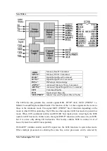
The bus controller chip has input lines S2*, S1*, S0* and CLK. These inputs to 8288 are
driven by CPU. It derives the outputs ALE, DEN, DT/R*, MRDC*, MWTC*, AMWC*,
IORC*, IOWC* and AIOWC*. The AEN, IOB and CEN pins are specially useful for
multiprocessor systems. AEN and IOB are generally grounded. CEN pin is usually tied to
+5V. The significance of the MCE/PDEN* output depends upon the status of the IOB pin. If
IOB is grounded, it acts as master cascade enable to control cascade 8259A, else it acts as
peripheral data enable used in the multiple bus configurations. INTA* pin used to issue two
interrupt acknowledge pulses to the interrupt controller or to an interrupting device. IORC*,
IOWC* are I/O read command and I/O write command signals respectively. These signals
enable an IO interface to read or write the data from or to the address port. The MRDC*,
MWTC* are memory read command and memory write command signals respectively and
may be used as memory read or write signals. All these command signals instructs the
memory to accept or send data from or to the bus. For both of these write command signals,
the advanced signals namely AIOWC* and AMWC* are available. They also serve the same
purpose, but are activated one clock cycle earlier than the IOWC* and MWTC* signals
respectively.
The maximum mode system timing diagrams are divided in two portions as read (input) and
write (output) timing diagrams. The address/data and address/status timings are similar to the
minimum mode. ALE is asserted in T1, just like minimum mode. The only difference lies in
the status signal used and the available control and advanced command signals.
Summary of Contents for 5586A
Page 2: ...Nvis 5586A Nvis Technologies Pvt Ltd 2...
Page 23: ...Nvis 5586A Nvis Technologies Pvt Ltd 23 Memory Read Timing in Maximum Mode...
Page 30: ...Nvis 5586A Nvis Technologies Pvt Ltd 30...
Page 48: ...Nvis 5586A Nvis Technologies Pvt Ltd 48 Diagram of module RESET power Instruction Set Note...

