background image


NXP Semiconductors 

AN10050


Designing a Hi-Speed USB host PCI adapter using ISP1562/63

AN10050_4 

© NXP B.V.  2007. All rights reserved.

Application note 

Rev. 04 — 1 November 2007 

5 of 18

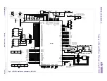
supply that pr5 V ± 5 % @ 2 A stabilized can be used. For example, a standard 
hub power supply. 

Note the distribution of pull-up resistors in the recommended schematics. For example, 
to achieve correct functionality, it is recommended that you connect the pull-up resistors 
placed on the PWEn_N and OCn_N input signals of the power switch, for example, 
MIC2026, to DV

AUX

 NET, maintaining a good condition of these signals even when  

+3.3 V and +5 V are off. The ‘fault flag’ pins (OCn_N) of MIC2026 are open-drain and 
require the presence of pull-up resistors. A 100 nF capacitor is used on each OCn_N 
signal to prevent false fault conditions. 

CLKRUN# is implemented in the ISP1562 on pin 42 and in the ISP1563 on pin 52. This 
signal is targeted mainly for mobile system designs. CLKRUN is an I/O pin. It is used by 
the system to safely turn-off the PCI CLK for power saving, with acknowledgment from 
the ISP1562/3 according to a predefined protocol. In the case of the PCI adapter card 
design, CLKRUN# must always be LOW because it is not present in the PCI connector. 
CLKRUN# may directly be connected to GND. For details on CLKRUN# function, refer to 

PCI Mobile Design Guide Version 1.1

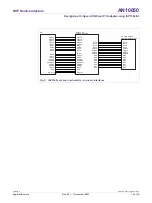
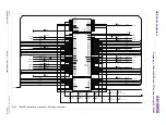
3.2  Input clock: applies only to the ISP1563 

You can use either of the following as clock input: 

• 

A 12 MHz crystal; the default recommended solution for best ElectroMagnetic 
Interference (EMI) results. 

• 

A 48 MHz oscillator; this may be a useful alternative, typically, in the case of on-
motherboard design. 

Both solutions for the input clock are shown in the schematics. 

To use a 48 MHz clock as input, connect the clock signal to the ISP1563 pin 86 (XTAL1), 
pin 87 (XTAL2) can be left open, and pin 121 (SEL48M) must be pulled up as shown in 
the schematics. 

In an add-on card configuration, normally, the 12 MHz crystal is used. In such a case, 
oscillators OSC2 and R45 are not necessary. Also, pin 121 (SEL48M) must directly be 
connected to GND. Another possibility is using a 12 MHz clock as an input. In this case, 
the 12 MHz-clock signal is directly connected to the ISP1563 pin 86 (XTAL1). This is 
similar to the case in which the 48 MHz clock is used; however, the ISP1563 pin 121 
must still be connected to GND. 

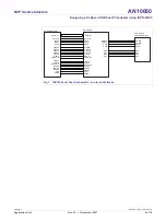
3.3  Selecting the number of ports: applies only to the ISP1563 

The selection of the number of ports, 2 or 4, is done using the SEL2PORTS signal 
(ISP1563 pin 5). It must be pulled to LOW, that is, connected to GND, for normal use of 
all four ports. If SEL2PORTS is HIGH, only two ports, that is, port 1 and port 2, are 
enabled; one port from each OHCI will be used in this case for performance 
improvement. Details regarding the power consumption and possible power savings in a 
two-port configuration can be found in the ISP1563 data sheet. 

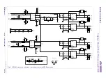
3.4  Subsystem vendor ID and subsystem device ID 

The ISP1562/3 allows loading of the Subsystem Vendor ID (VID) and the Subsystem 
Device ID (DID) for both EHCI and OHCI from an external EEPROM. Loading of these 
values in the configuration registers of the ISP1562/3 will occur only if a value of 15h is 
found in byte 7 of the EEPROM. The necessary signals, I

2

C-bus clock and I

2

C-bus data, 

Summary of Contents for ISP1562

Page 1: ...SP1563 Rev 04 1 November 2007 Application note Document information Info Content Keywords isp1562 isp1563 usb universal serial bus host pci adapter Abstract This document contains a description of the...

Page 2: ...or additional information please visit http www nxp com For sales office addresses please send an email to salesaddresses nxp com Revision history Rev Date Description 04 20071101 Fourth revision Corr...

Page 3: ...t controller device driver interacts with these registers to implement the USB functionality and the legacy support A detailed description of configuration registers and operational registers can be f...

Page 4: ...ct the presence of PCI VAUX 3 3 V and automatic selection of the input voltage Selection of PCI VCC 3 3 V must be the default position of jumper JP1 in the case of a standard add on card design The ot...

Page 5: ...ference EMI results A 48 MHz oscillator this may be a useful alternative typically in the case of on motherboard design Both solutions for the input clock are shown in the schematics To use a 48 MHz c...

Page 6: ...ve USB port is signaled to the ISP1562 3 by the external port power switching device The fault condition that is usually signaled by an external power switching device can be an overcurrent or a therm...

Page 7: ...he clearance imposed by the manufacturing process around any via holes to an internal plane Try to keep the length of the DP and DM traces equal The maximum trace length mismatch between high speed US...

Page 8: ...as possible to the USB connector Special attention must be given when placing additional components on the DP and DM lines and routing recommendations must be followed Both VDDA_AUX analog and VCC I...

Page 9: ...NNECTOR AD 31 0 PCICLK RST IDSEL GNT C BE0 C BE1 C BE2 C BE3 INTA REQ FRAME TRDY IRDY DEVSEL STOP PERR SERR PAR PME AD 31 0 PCICLK RST IDSEL GNT C BE0 C BE1 C BE2 C BE3 INTA REQ FRAME TRDY IRDY DEVSEL...

Page 10: ...23 AD 24 AD 25 AD 26 AD 27 AD 28 AD 29 AD 30 AD 31 AD0 AD1 AD2 AD4 AD3 70 69 68 67 66 65 AD5 AD6 63 AD7 AD8 AD9 AD10 AD11 AD12 AD13 AD14 AD15 AD16 AD17 AD18 AD19 AD20 AD21 AD22 AD23 AD24 AD25 AD26 AD2...

Page 11: ...5 12 V TCK GND TDO 5 V 5 V INTB INTD PRSNT 1 RESERVED PRSNT2 TRST 12 V TMS TDI 5 V INTA INTC 5 V RESERVED VIO RESERVED B14 B15 B16 B17 B18 B19 B20 B21 B22 B23 B24 B25 B26 B27 B28 B29 B30 B31 B32 B33 B...

Page 12: ...V Optional J1 1 2 3 5 VBUS C5 47 F 10 V C7 0 1 F C6 100 pF 5 6 7 8 R20 560 LED D2 C1 0 01 F C2 47 F 10 V C3 1 nF C4 22 F 10 V C41 0 1 F 5 VBUS FB8 BLM41PG600SN1 D1 LED 5V_Standby A TT1 TT2 B 5 V C42 0...

Page 13: ...E2 C BE3 INTA REQ FRAME TRDY IRDY DEVSEL STOP PERR SERR PAR PME PWE3 PWE4 DM1 DM2 DP2 ISP1563_ES1 ISP1563_ES1 SCH POWER_SWITCH POWER_SWITCH SCH RST GNT AD 31 0 PCICLK IDSEL C BE0 C BE1 C BE2 C BE3 INT...

Page 14: ...C BE 2 C BE 3 PCICLK IDSEL GNT AMB1 INTA REQ FRAME TRDY IRDY DEVSEL STOP PERR SERR PAR PME RST CLKRUN AMB2 AMB3 AMB4 GRN1 GRN2 GRN3 GRN4 OC1_N OC2_N OC3_N OC4_N PWE1_N PWE2_N PWE3_N PWE4_N DM1 DM2 DM...

Page 15: ...2 V TCK GND TDO 5 V 5 V INTB INTD PRSNT 1 RESERVED PRSNT2 TRST 12 V TMS TDI 5 V INTA INTC 5 V RESERVED VIO RESERVED B14 B15 B16 B17 B18 B19 B20 B21 B22 B23 B24 B25 B26 B27 B28 B29 B30 B31 B32 B33 B34...

Page 16: ...USB1 IP 4220CZ6 1 2 3 4 6 5 ESD1 DM1 DM1 DP1 DP2 R17 15 k R18 15 k DP1 C7 0 1 F C56 220 F 10 V C44 1 nF FB3 BLM18PG121SN1 VBUS GND SHIELD SHIELD D D CON2 USB2 1 4 6 2 3 5 1 2 3 4 5 6 IP 4220CZ6 ESD2 R...

Page 17: ...in this document including without limitation specifications and product descriptions at any time and without notice This document supersedes and replaces all information supplied prior to the publica...

Page 18: ...se 1 November 2007 Document identifier AN10050_4 7 Contents 1 Introduction 3 2 ISP1562 3 initialization 3 3 Description of the application schematics 4 3 1 Distribution of power sources and power mana...

Reviews: