2-3
CHAPTER 2 THEORY OF OPERATION
2.3
PRINTED CIRCUIT BOARD DESCRIPTION
( See Block Diagram Figure 2-3 and Schematic Diagram, Figure 5-2)
2.3.1 Power Supply
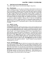
Power is supplied to the unit from either an AC Adapter which provides 9 volts dc or an
internal 9 volt Alkaline battery. External power is supplied through a jack mounted at
the rear of the balance. Diode D9 is a protection diode which prevents the wrong polarity
voltage from being applied to the balance. Capacitor C18 is a filter which is used to filter
the raw dc voltage coming from the external power supply or battery. Capacitor C8 is
a transient suppressor. The power input jack J3 has a contact which disconnects the
internal 9 volt battery when the AC Adapter is connected to the balance. The Printed
Circuit Board contains one voltage regulator VR1 (LM2930) which provides a regulated
+ 5 volts dc to operate the balance. Filtering of the +5 volts dc is accomplished by
capacitors C14 and C9. Transistor Q6 which is in series with voltage regulator VR1
applies dc power to the regulator and is part of the ON/OFF circuit function which is
described in paragraph 2.3.2. Transistor Q6 must be on in order for the voltage regulator
to operate.
2.3.2 ON/OFF Circuitry
2.3.2.1 Turn On Circuitry
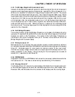
The ReZero On switch SW1 performs two functions, one is to turn the balance on and
the second is for taring the balance. When the balance is properly connected to a power
source, pressing ReZero On switch SW1 applies a ground through diode D6, resistor
R22 to the base of transistor Q6 and turns on transistor Q6. When microprocessor U1
receives power, an "on" signal is generated at pin 18 of the microprocessor and is
passed through resistor R20 to the base of transistor Q5. Transistor Q5 has a current
path through resistors R21 and R41, turns on and acts as a latch and keeps transistor
Q6 turned on. When ReZero On switch SW1 is released, transistor Q6 remains on.
Transistor Q6 is in series with voltage regulator VR1. If transistor Q6 is not turned on,
voltage regulator VR1 will not operate. With transistor Q6 turned on, VR1 is operational
and provides a reg5 volts dc output. When ReZero On switch SW1 is pressed,
a ground signal is also applied to diode D7. Diode D7 passes the ground signal to
microprocessor U1 on pin 9.
2.3.2.2 Turn Off Circuitry
Pressing and holding Mode Off switch SW2 turns the balance off by ap5 volts
dc to microprocessor U1 pin 8. When this occurs, the display will indicate OFF and the
signal generated by the microprocessor to resistor R20 goes low to transistor Q5 turning
off transistors Q5 and Q6. The microprocessor generated signal on resistor R20 takes
about one second. In the event that the microprocessor locks up, pressing and holding
Mode Off switch SW2 for five seconds or more a5 volts dc to resistors R37, R39
and charges capacitor C16 which turns on transistor Q1. With transistor Q1 on,
transistor Q5 is turned off and transistor Q6 turns off thus removing dc power from
voltage regulator VR1 and all dc power from the balance.
Summary of Contents for SCOUT
Page 1: ...OhausCorporation 29HanoverRoad FlorhamPark NJ 07932 0900 ELECTRONIC BALANCES SERVICE MANUAL TM...
Page 6: ...i v...
Page 10: ...1 4 CHAPTER 1 INTRODUCTION...
Page 38: ...5 2 CHAPTER 5 DRAWINGS AND PARTS LISTS...
Page 39: ...5 3 CHAPTER 5 DRAWINGS AND PARTS LISTS Figure 5 1 Exploded View of Balance 5 3 5 4...
Page 43: ...SCOUT ELECTRONIC BALANCES P N 300040 010 R1198...
Page 45: ...e e e...
Page 47: ......


