40055101TH Rev.4
369 /
A2.1
Explanation of Signal Flow for OKIOFFICE44/OKIFAX 4100/5000 Series
Note : Regarding the difference of the signal flow between OKIFAX 4100 and OKIFAX 5000 series,
since one-line scanning processing speed of OKIFAX 5000 series is faster in comparison with
OKIOFFICE 44/OKIFAX 4100, to the circuit diagram of OKIFAX 5000 series has been added
the EXSEED (image processing LSI) and SRAM (dark/light level correction data). Otherwise,
the signal flow is almost the same as in OKIOFFICE 44/OKIFAX 4100.
(1)
Copy Mode
•
Copy mode for OKIOFFICE 44/OKIFAX 4100
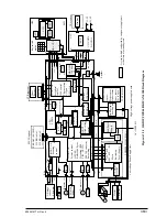
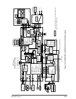
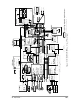
Figure A2.1.1 shows the picture signal route in local copy mode for OKIOFFICE 44/OKIFAX
4100
One-line picture data is transferred to A/D converter (analog/digital converter) from the
scanning unit (CIS: contact image sensor) as an analog data. After conversion from analog
data to 6-bit digital data by A/D converter, the picture data is sent to DRAM (line memory) via
IOGA by DMA (Direct Memory Access). Then the picture data is sent to IOGA again. Here,
the picture data undergoes various kinds of picture processings (IOGA and CPU), and is
converted to two-level binary data (black and white). The one-line binary data from IOGA is
stored into DRAMs (page memory). When the data for one page has been stored in the
DRAMs, the data is read out from the DRAMs and sent to IOGA. The data is converted into a
serial data by the picture control of IOGA and transferred to the LED print head for printing as
HDATA 0/1. Writing of data into the page memory is also possible during the printing
operation.
•
Copy mode for OKIFAX 5000 series
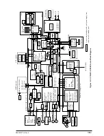
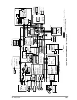
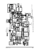
Figure A2.2.1 shows the picture signal route in local copy mode for OKIFAX 5000 series
One-line picture data is transferred to A/D converter (analog/digital) via operational amplifier
from the scanning unit (CIS: contact image sensor) as an analog data. After conversion from
analog data to 6-bit digital data by A/D converter, the picture data is sent to EXSEED (image
processing LSI) and SRAM. Here, the picture data undergoes various kinds of picture
processings (EXSEED and SRAM), converted to two-level binary data (black and white) and
then sent to IOGA (scanning control). The one-line binary picture data from IOGA is stored
into DRAM. When the data for one page has been stored in the DRAM, the data is read out
from the DRAM and sent to IOGA. The data is converted into a serial data by the picture
control of IOGA and transferred to the LED print head for printing as HDATA. Writing of
data into the page memory is also possible during the printing operation.
(2) G3 Send Mode
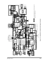
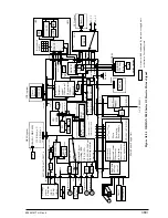
Figure A2.1.2 (For OKIOFFICE 44/OKIFAX 4100)/Figure A2.2.2 (For OKIFAX 5000 series)
show the G3 send picture signal route
In the G3 mode, the data transfer route from the scan unit up to the DRAM is the same as in the
copy mode described in (1).
The picture data for one-line is transferred from DRAM to CPU. The CPU performs the picture
data processing (encode) for this picture data (FILLER, fill bits are inserted etc.) and again stores
into the DRAM. The stored encoded data is output from DRAM to the MODEM under the
control of CPU. After modulation, the picture signal “S” is sent to the NCU board as the trans-
mission data. The transmission data “S” goes through the amplifier and is sent to the telephone
line L1 and L2 via the transformer T1 as high speed signal.
Summary of Contents for B4100
Page 73: ...40055101TH Rev 4 73 2 For OKIFAX 5000 series AC Power Switch AC Inlet FX050VP C2 014...
Page 158: ...40055101TH Rev 4 158 Appearance of the OKIOFFICE44 OKIFAX 4100 FX048 CP4 1 Fig 01...
Page 461: ...40055101TH Rev 4 461...
Page 462: ...40055101TH Rev 4 462...
Page 463: ...40055101TH Rev 4 463...
Page 464: ...40055101TH Rev 4 464...
Page 465: ...40055101TH Rev 4 465...
Page 466: ...40055101TH Rev 4 466...
Page 467: ...40055101TH Rev 4 467...
Page 468: ...40055101TH Rev 4 468...
Page 469: ...40055101TH Rev 4 469...
Page 470: ...40055101TH Rev 4 470...
Page 471: ...40055101TH Rev 4 471...
Page 472: ...40055101TH Rev 4 472...
Page 473: ...40055101TH Rev 4 473...
Page 545: ...40055101TH Rev 4 545 54 SECTION 1 CABINET ASSEMBLY FAX NIP FX048...
Page 548: ...40055101TH Rev 4 548 SECTION 2 UNIT PRINTER...
Page 550: ...40055101TH Rev 4 550 SECTION 3 UNIT 048 OPE PANEL...
Page 552: ...40055101TH Rev 4 552 SECTION 4 OPEPANEL OPERATION PANEL ASSEMBLY...
Page 554: ...40055101TH Rev 4 554 SECTION 5 FRAME ASSEMBLY SCANNER L...
Page 556: ...40055101TH Rev 4 556 SECTION 6 PLATE ASSEMBLY SCANNER B...
Page 558: ...40055101TH Rev 4 558 SECTION 7 PLATE ASSEMBLY SCANNER R...
Page 560: ...40055101TH Rev 4 560 17 16 15 10 SECTION 8 FRAME ASSEMBLY SCANNER U...
Page 562: ...40055101TH Rev 4 562 13 SECTION 9 COVER ASSEMBLY TOP...
Page 564: ...40055101TH Rev 4 564 SECTION 10 PLATE ASSEMBLY BASE...
Page 569: ...40055101TH Rev 4 569 SECTION 12 PRINTER HEAT ASSY...
Page 571: ...40055101TH Rev 4 571 SECTION 13 CABLES...
Page 574: ...40055101TH Rev 4 574 SECTION 1 CABINET ASSEMBLY...
Page 576: ...40055101TH Rev 4 576 SECTION 2 CONTROL PANEL ASSEMBLY OKIFAX 5200 5300...
Page 577: ...40055101TH Rev 4 577 SECTION 2 CONTROL PANEL ASSEMBLY OKIFAX 5500 5600...
Page 579: ...40055101TH Rev 4 579 SECTION 3 PRINTER ASSEMBLY...
Page 582: ...40055101TH Rev 4 582 SECTION 4 BASE ASSEMBLY 30 37 38...
Page 585: ...40055101TH Rev 4 585 SECTION 5 SCAN UNIT...
Page 587: ...40055101TH Rev 4 587 SECTION 6 PAPER GUIDE U ASSEMBLY...
Page 589: ...40055101TH Rev 4 589 SECTION 7 CABLES 10...
Page 591: ...40055101TH Rev 4 591 SECTION 8 OPTION TELEPHONE US...
Page 594: ...40055101TH Rev 4 594 SECTION 8 OPTION TELEPHONE UK ITA NOR DEN BEL...
Page 597: ...40055101TH Rev 4 597 SECTION 8 OPTION TELEPHONE HOL GER FRA SWITZ AUT INT L...

