40055101TH Rev.4
386 /
A3.1.3
R44 Circuit Diagram (Page 3/12)
1.
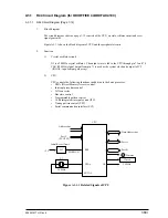
Block diagram
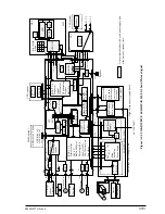
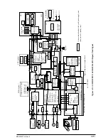
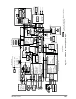
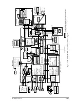
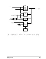
The circuit diagram shown on page 3/12 consists of Flash memory, Mask ROM, DRAM, Real
time clock IC and Back up battery circuit.
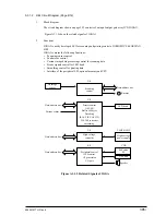
Figure A3.1.3 shows the block diagram of Flash memory, Mask ROM, DRAM and Real time
clock.
2.
Function
1)
Flash memory (FLS1)
Flash memory (electrically erasable and programmable device) is used for the main
software program, which is stored in EP-ROM of the current OKIFAX. Other than the
function of EP-ROM, Flash memory is also used for the user data area instead of SRAM
chips.
•
512 KByte Flash memory x 1 (FLS)
Used for work area, report recording etc.
2)
Mask ROM
3)
DRAM
512 KByte DRAM x 2 (RAM1 and RAM2)
•
Used as follows:
Picture memory for the ECM send/receive mode.
Picture memory for the memory transmission mode.
Picture memory for the retransmission mode.
Picture memory for the reception in memory.
Editing for report printing.
4)
Back-up battery circuit
The non-rechargable lithium battery supplies voltage to a real-time clock IC at AC main
interruption.
5)
Real-time clock IC (IC3)
IC3 is a real-time clock IC used as a timepiece to display the data and time in year, month,
day, hour, minute, and second units. Its input/output signals are the 4-bit data bus (AD00 -
AD03), 4-bit address bus (A01 - A04) and the control signals, RTCCS, MDMRD-N and
MDWR-N which perform a CPU-controlled read operation (M/D/Y H:M, Data read) and
write operation (M/D/Y H:M, Data setting).
Summary of Contents for B4100
Page 73: ...40055101TH Rev 4 73 2 For OKIFAX 5000 series AC Power Switch AC Inlet FX050VP C2 014...
Page 158: ...40055101TH Rev 4 158 Appearance of the OKIOFFICE44 OKIFAX 4100 FX048 CP4 1 Fig 01...
Page 461: ...40055101TH Rev 4 461...
Page 462: ...40055101TH Rev 4 462...
Page 463: ...40055101TH Rev 4 463...
Page 464: ...40055101TH Rev 4 464...
Page 465: ...40055101TH Rev 4 465...
Page 466: ...40055101TH Rev 4 466...
Page 467: ...40055101TH Rev 4 467...
Page 468: ...40055101TH Rev 4 468...
Page 469: ...40055101TH Rev 4 469...
Page 470: ...40055101TH Rev 4 470...
Page 471: ...40055101TH Rev 4 471...
Page 472: ...40055101TH Rev 4 472...
Page 473: ...40055101TH Rev 4 473...
Page 545: ...40055101TH Rev 4 545 54 SECTION 1 CABINET ASSEMBLY FAX NIP FX048...
Page 548: ...40055101TH Rev 4 548 SECTION 2 UNIT PRINTER...
Page 550: ...40055101TH Rev 4 550 SECTION 3 UNIT 048 OPE PANEL...
Page 552: ...40055101TH Rev 4 552 SECTION 4 OPEPANEL OPERATION PANEL ASSEMBLY...
Page 554: ...40055101TH Rev 4 554 SECTION 5 FRAME ASSEMBLY SCANNER L...
Page 556: ...40055101TH Rev 4 556 SECTION 6 PLATE ASSEMBLY SCANNER B...
Page 558: ...40055101TH Rev 4 558 SECTION 7 PLATE ASSEMBLY SCANNER R...
Page 560: ...40055101TH Rev 4 560 17 16 15 10 SECTION 8 FRAME ASSEMBLY SCANNER U...
Page 562: ...40055101TH Rev 4 562 13 SECTION 9 COVER ASSEMBLY TOP...
Page 564: ...40055101TH Rev 4 564 SECTION 10 PLATE ASSEMBLY BASE...
Page 569: ...40055101TH Rev 4 569 SECTION 12 PRINTER HEAT ASSY...
Page 571: ...40055101TH Rev 4 571 SECTION 13 CABLES...
Page 574: ...40055101TH Rev 4 574 SECTION 1 CABINET ASSEMBLY...
Page 576: ...40055101TH Rev 4 576 SECTION 2 CONTROL PANEL ASSEMBLY OKIFAX 5200 5300...
Page 577: ...40055101TH Rev 4 577 SECTION 2 CONTROL PANEL ASSEMBLY OKIFAX 5500 5600...
Page 579: ...40055101TH Rev 4 579 SECTION 3 PRINTER ASSEMBLY...
Page 582: ...40055101TH Rev 4 582 SECTION 4 BASE ASSEMBLY 30 37 38...
Page 585: ...40055101TH Rev 4 585 SECTION 5 SCAN UNIT...
Page 587: ...40055101TH Rev 4 587 SECTION 6 PAPER GUIDE U ASSEMBLY...
Page 589: ...40055101TH Rev 4 589 SECTION 7 CABLES 10...
Page 591: ...40055101TH Rev 4 591 SECTION 8 OPTION TELEPHONE US...
Page 594: ...40055101TH Rev 4 594 SECTION 8 OPTION TELEPHONE UK ITA NOR DEN BEL...
Page 597: ...40055101TH Rev 4 597 SECTION 8 OPTION TELEPHONE HOL GER FRA SWITZ AUT INT L...


