40838301TH Rev.1
7 - 26
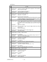
9
Probable cause 1: D85 is defective.
Check item 1:
Replace D85.
Probable cause 2: The load is larger than the normal value.
Check item 2:
Check if the load current is 2
µ
A or less.
Probable cause 3: D52 is defective.
Check item 3:
Check if D52 is iZ300 class Y or Z (class X is not acceptable).
10
Probable cause 1: Q11 and Q12 are malfunctioning.
Check item 1:
Check the PWM waveform of DB output (cycle: 142
µ
s, ON time: 36
µ
s).
Check item 2:
Check Q11 and Q12. Check the base voltage of Q21, Q22 and Q23 (3.7V
or more to 3.9V or more).
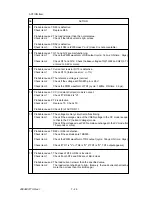
11
Probable cause 1: Current set resistor R115 is defective.
Check item 1:
Check R115 (tolerance error: +/-1%)
Probable cause 2: The reference voltage is incorrect.
Check item 2:
Check if the voltage at CN3-B10 pin is 2.5V.
Check item 3:
Check the PWM waveform of TR1 (cycle: 142Ms, ON time: 36
µ
s).
12
Probable cause 1: CC (Constant Current) mode is not set.
Check item 1:
Check if TR SEL2 is "H".
Probable cause 2: T2 is defective.
Check item 2:
Replace T2. Check T2.
Probable cause 3: Check (3) of ACTION 11.
13
Probable cause 1: The voltage memory circuit is malfunctioning.
Check item 1:
Check if the average value of the VSEN voltage in the CC mode is equal
to that in the CV (Current Voltage) mode.
Check if the voltage across C230 remains unchanged in the CV mode (for
15 seconds or more).
14
Probable cause 1: D65 or D66 is defective.
Check item 1:
Check if these diodes are 1ZB390.
Check item 2:
Check the PWM waveform of TR2 output (cycle: 146
µ
s, ON time: 36
µ
s).
Check item 3:
Check if TR1 is "L" or TR2 is "H" (if TR1 is "H", TR1 output appears).
15
Probable cause 1: The class of D76 or D82 is incorrect.
Check item 1:
Check if both D76 and D82 are of EB-2 class.
Probable cause 2: The load current is lower than the specified value.
Check item 2:
The load current shall be 6 to 8
µ
A. (Namely, the load current shall not be
more than or less than this limit range.)
ACTION Item:
No.
ACTION
Summary of Contents for OKIFAX 5400
Page 7: ...40838301TH Rev 1 CHAPTER 1 GENERAL INFORMATION...
Page 46: ...40838301TH Rev 1 CHAPTER 2 INSTALLATION PROCEDURE...
Page 130: ...40838301TH Rev 1 CHAPTER 3 BRIEF TECHNICAL DESCRIPTION...
Page 138: ...40838301TH Rev 1 CHAPTER 4 MECHANICAL DISASSEMBLY AND REASSEMBLY...
Page 157: ...40838301TH Rev 1 CHAPTER 5 ADJUSTMENTS...
Page 162: ...40838301TH Rev 1 CHAPTER 6 CLEANING AND MAINTENANCE...
Page 189: ...40838301TH Rev 1 CHAPTER 7 TROUBLESHOOTING AND REPAIR FOR OKIFAX 5400...
Page 240: ...40838301TH Rev 1 CHAPTER 8 DIPSWITCHS SETTING TABLES...
Page 380: ...40838301TH Rev 1 D 2 SECTION 1 CABINET ASSEMBLY 5...
Page 382: ...40838301TH Rev 1 D 4 SECTION 2 CONTROL PANEL ASSEMBLY...
Page 384: ...40838301TH Rev 1 D 6 SECTION 3 PRINTER ASSEMBLY 51...
Page 387: ...40838301TH Rev 1 D 9 SECTION 4 BASE ASSEMBLY 30 37 36 39 40 5...
Page 390: ...40838301TH Rev 1 D 12 SECTION 5 SCAN UNIT...
Page 392: ...40838301TH Rev 1 D 14 SECTION 6 PAPER GUIDE U ASSEMBLY...
Page 394: ...40838301TH Rev 1 D 16 SECTION 7 CABLES 10 11 19 12 20 21...
Page 396: ...40838301TH Rev 1 D 18 SECTION 8 OPTION TELEPHONE US...
Page 399: ...40838301TH Rev 1 D 21 SECTION 8 OPTION TELEPHONE UK ITA NOR DEN BEL...
Page 402: ...40838301TH Rev 1 D 24 SECTION 8 OPTION TELEPHONE HOL GER FRA SWITZ AUT INT L...

