


FM Transmitter
Sistemas Electrónicos S.A EM 250 COMPACT DIG
Technical Manual - v1.1 - February 2006
31
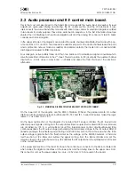
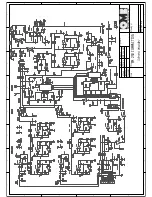
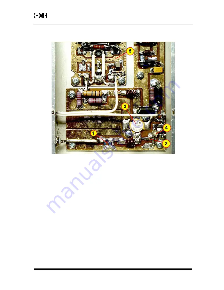
Detailed views of the three sections composing the Power Amplifier module are shown in Figures 2-4,
2-5 and 2-6 below:
Fig. 2-4: DETAILED VIEW OF INPUT DRIVER STAGE.
Figure 2-4 above shows a magnified view of RF driver stage, a BLF 242 transistor working in class AB
configuration. Numbered elements corresponds to the following description:
1
- Input matching attenuator circuit.
2
- BLF 242 RF Driver transistor.
3
- Bias control circuit.
4
- Input impedance-matching transformer.
5
- Output power amplifier stage PC board.
A resistive input attenuator (1), when present, enhances matching with the preceding unit and
contributes to insulate the two stages. After that, a broadband matching network feeds the transistor
gate.
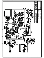
Output amplifier stage detail can be seen in Figure 2-5.


