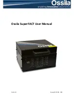
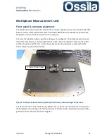
background image


Ossila Ltd 


Copyright © 2009 - 2015 


Ossila SuperFACT User Manual 


Summary of Contents for FACT1

Page 1: ...Ossila Ltd Copyright 2009 2015 Ossila SuperFACT User Manual ...

Page 2: ... INTRODUCTION TO FIELD EFFECT TRANSISTORS 33 OUTPUT CHARACTERISTIC I V 35 TRANSFER CHARACTERISTIC TC 36 GATE DEPENDENT MOBILITY 38 TRANSFER CHARACTERISTIC CURVES IDEAL AND REAL BEHAVIOUR 39 THRESHOLD VOLTAGE SECOND DERIVATIVE METHOD 40 FIGURES OF MERIT 41 WELL BEHAVED TRANSISTOR AND VALIDATION OF THE FIGURES OF MERIT 42 QUICK START 43 DATA ANALYSIS 48 SAVE EXPERIMENT SETTINGS 49 DELETE AN EXISTING...

Page 3: ... ACCURACY 86 TEMPERATURE AND SELF CALIBRATION 86 CALCULATION OF THE MEASUREMENT ACCURACY 86 TEMPERATURE EFFECTS ON SMU ACCURACY 88 LIST OF SYMBOLS AND ACRONYMS 89 SUPERFACT TROUBLESHOOTING 90 GUIDE TO THE READER SYMBOLS ACRONYMS AND COMMON DEFINITIONS 94 WARRANTY INFORMATION AND CONTACT DETAILS 95 APPENDICES 96 APPENDIX I CLEANING ROUTINE 96 APPENDIX II PMMA GATE DIELECTRIC 97 APPENDIX III PEDOT P...

Page 4: ...the twenty devices on the substrate SuperFACT multiplexor makes use of a 2D array of gold coated spring loaded probes POGOS to connects the devices to the source meter s while the transistor to measure are selected through a high performance switching network At the core of the measurement system is a computer controlled Keithley dual source measure unit with maximum output of 100 V and accuracy u...

Page 5: ... to conserve the accuracy of the measurement If not using the Ossila SuperFact controlled Software ensure the Drain and Gate input signals are limited to 100 mA Caution To avoid damaging devices or equipment obey the following Avoid electrostatic discharge ESD as this may damage the device To avoid damage use static discharge and prevention equipment where necessary Only use the System for the pur...

Page 6: ...12B system SMU Ossila Multiplexer Measurement Unit containing NI USB 6501 OEM electronic controls LED display and the signal board supporting POGO pin contacts probes for 20 devices and 8 gates Desktop PC Window 8 1 operative system endowed with Core i7 Intel microprocessors 24 Monitor Keyboard ...

Page 7: ...ent and of the Council and directive 2006 95 EC of the European Parliament and of the Council Mouse Two flexible coaxial cables endowed with BNC and I O connectors One USB cables with Standard A and Standard B plugs on the opposite ends One GPIB cable with USB connectors Also included Three Power Supply Leads Cords for the monitor computer and the SMU ...

Page 8: ...itive test and measurement equipment for EMC unprotected applications IEC 61326 2 1 2005 2006 95 EC EN 61010 1 2010 Safety requirements for electrical equipment for measurement control and laboratory use Part 1 General requirements IEC 61010 1 2010 EN 61010 2 030 2010 Safety requirements for electrical equipment for measurement control and laboratory use Part 2 030 Particular requirements for test...

Page 9: ...ential Requirements of the Directives Signed Name Dr James Kingsley Date System Setup The Multiplexer Measurement Unit is easy and straightforward to set up Only a few cable connections are required to make the system fully operational Nonetheless the User must read carefully the following instructions in order to safely and efficiently exploit the performance and accuracy of the Ossila Multiplexe...

Page 10: ... or affect the performance of the device In addition you must read the Keithley 2612B System SMU manuals first which are provided with the SMU with particular reference to the Safety information Do not operate any third party devices outside the operational range specified by their respective manufacturers Ossila must not be held responsible for any injury or damage due to the non strict observanc...

Page 11: ...cables to double check the connections 4 Use the USB cable provided to connect the Multiplexer Measurement Unit with the computer case To do this plug the Standard B USB plug to the Standard B USB receptacle located on the back panel of the Unit see figure 1 Plug the Standard A USB end of this cable to any USB 2 0 or higher socket on the computer casing The USB socket must be capable of delivering...

Page 12: ...enabling innovative electronics Ossila Ltd Copyright 2009 2015 12 Figure 1 USB cable and coaxial cables BNCs connection Channel A is the Gate Channel B is the Drain ...

Page 13: ...m for further information on installing and using the executable on a target computer already running Labview Required drivers 1 LabVIEW Run Time Engine 2014 or later version 2 NI 488 2 Application Development Support 14 0 or later version1 3 NI DCPower Development Support only for NI PXI 4132 SMU 2 4 NI DAQmx Runtime with configuration support 5 NI System Configuration Runtime 6 NI Measurement Au...

Page 14: ...using Windows 7 8 8 1 or later distributions you must enable the application to write the data folder To change the data folder access permission Navigate to C Programme Files 86X SuperFACT and right click the data folder On the drop down menu click on Properties and on tab menu of select Security Under Group or user names select the relevant PC user Click on edit and make sure that Full control i...

Page 15: ... in the new data folder and replace them with the entirety of the file in the data folder with the exception of the ddl file otherwise the application may stop working properly Alternatively before re installing the application delete the data folder to delete any previous reference to old experiment settings ...

Page 16: ...ure 2 The holder consists of a push fit bracket and a 2D array of twenty eight POGO probes When a substrate is placed in the holder with the lid secured with its four screws the probes provide low resistance contact with all the device and gate pads on the substrate Figure 2 Substrate holder containing twenty Drain Source probes and eight Gate probes The Gate connections are provided by the bottom...

Page 17: ...corresponding Gate probe connects it to the signal generated by the GATE SMU Figure 4 shows which column of POGOS are Drain or Source probes Figure 4 Location of Signal and Source Drain probes for Dev 16 The first column on the left therefore acts as the Source ground while the second is used to apply the desired voltage Drain to the transistors This pattern alternate Source and Drain columns repe...

Page 18: ...DRAIN or GATE SMU The Device and Gate LEDs arrangement matches exactly with the Device and Gate layout on the substrate see figure 4 Conversely as the substrate is placed face down on the POGOS the position of the probes is a flipped version of the device location on the substrate see figure 5 Figure 5 Front panel of the Multiplexer Measurement Unit corresponds to location of the transistor on the...

Page 19: ...panel The back panel houses the coaxial connections for the Drain channel B and Gate channel A the USB B socket for the USB cable and the earthing pin see figure 6 There is also an earthing cable to earth the chassis Figure 6 Back panel of the Multiplexer Measurement Unit ...

Page 20: ... and 100 V respectively These limits should be hard coded in the control software so that no user can unintentionally supply read voltages currents whose values are outside the operational range of the multiplexer If using alternative software is the software engineer programmer is responsible for testing whether the application is working correctly and the SMU is operating within the limit descri...

Page 21: ...rtant The maximum current that the USB can supply to the multiplexor relay network limits the number of lines Drains and Gates that can be switched and maintained on to twenty two For lifetime and stress biased measurements it is recommended to connect the USB cable using a USB power adapter version 3 0 or later to ensure continuous operation Please note that the coaxial cables used to connect the...

Page 22: ...R 0 7 Ω C 278 pF Dev 15 R 0 8 Ω C 281 pF Dev 20 R 0 8 Ω C 286 pF Dev 4 R 0 51 Ω C 270 pF Dev 9 R 0 6 Ω C 273 pF Dev 14 R 0 6 Ω C 274 pF Dev 19 R 0 7 Ω C 286 pF Dev 3 R 0 6 Ω C 275 pF Dev 8 R 0 7 Ω C 274 pF Dev 13 R 0 9 Ω C 286 pF Dev 18 R 0 8 Ω C 285 pF Dev 2 R 0 6 Ω C 283 pF Dev 7 R 0 7 Ω C 280 pF Dev 12 R 0 8 Ω C 283 pF Dev 17 R 0 8 Ω C 286 pF Dev 1 R 0 5 Ω C 272 pF Dev 6 R 0 6 Ω C 277 pF Dev 11...

Page 23: ...ox required ANSI C LabWindows CVI Measurement Studio Visual Basic Visual Studio Visual Studio NET In order for the Ossila Multiplexer Measurement Unit to be recognised by your computer please ensure that the National Instruments DAQmx driver version 14 or above is installed on your system Many computers running LabVIEW with other national instruments hardware will already have DAQmx drivers instal...

Page 24: ... USB 6501 input ouput signal is constituted of 24 independent DIO lines or channels arranged in three groups of eight Four DIO lines P0 0 P0 1 P0 2 and P0 3 are assigned to select to a particular Device column see figure 8 while the DIO lines used to address each single Device are shared between two columns For example Dev 1 is controlled by the column line P0 0 and row line P0 4 while Dev 16 is t...

Page 25: ...ly one Device is to be turned on at a time as the current or voltage to be measured is accesed via Channel B However the Multiplexer Measuring Unit can also be used for stress biased measurement whereby all the Devices are switched on see section Operation Table 2 Digital DIO channels controlling the Multiplexer Measurement Unit Port Signal Name Direction software selectable Description Port 0 P0 ...

Page 26: ...es and virtual instruments Execute system diagnostics View devices and instruments connected to your system Update your National Instruments software In the following we refer to the Source Measurement Units SMU dedicated to source and measure the gate and drain voltage current of transistor as GATE and DRAIN respectively Gate and drain lower case letter refers to the transistor gate and drain res...

Page 27: ... on the alias name select Rename on the drop down menu and input the new alias 3 Familiarise with the tool bar commands on the central subpanel of MAX see figure 14 4 Use Reset to reset the hardware and Self Test to test the hardware Stress Biased Measurement Figure 9 SwitchControl NI USB 6501 MAX front panel ...

Page 28: ...The current specifications of the NI USB 6501 limits the number of Drains and Gates that can be switched ON to 22 see figure 10 Due to the topology of the multiplexer network only the following operations are possible 1 Switch on off a single device 2 Switch on off all the devices of a column 3 Switch on off all the devices of a row 4 Switch on off devices pairs The pairs in point 4 are the ones t...

Page 29: ... GBIP for Keithley and NI PXI 8360 for PXI alias names must be assigned to the SMU and peripheral units through NI MAX Measurement Automation Explorer 5 5 If MAX is not yet installed please download and install it MAX is freely available at www ni com registration to NI website may be required to download NI applications and drivers Figure 11 Any number of Device column or rows can be switched off...

Page 30: ...s entry to show the drop down menu options Select Rename and rename Dev1 as SwitchControl20 this name is case sensitive For Keithley SMU In Devices and Interfaces search for the GBIP device and with the mouse left click to expand the list of devices connected to the target PC through the GBIP interface If the list is empty on the control bar located on the top side of MAX right panel click on Scan...

Page 31: ...installed on the host computer see SuperFACT Software Installation Figure 12 MAX Measurement Automation Explorer user interface Operation Mode SuperFACT can automatically acquire OFET TFT output and transfer characteristics of a multi device substrate by switching between the different channels of a multiplexor with each channel pogo being connected to a different device Alternatively if a manual ...

Page 32: ...Mode automatically Important Do not use the multiplexer in manual mode When in manual mode the multiplexer unit remains inactive throughout the acquisition cycle However providing the host computer is connected to the multiplexer it is possible to take measurement using a manual text fixture in manual mode In this case you need to connect the SMU to the manual test fixture manually select the devi...

Page 33: ...finite The transistor figures of merit are stored as time series on a single csv file per device Combine Measurement Modes The user can combine bias acquisition with continuous measurement in order to carry out lifetime experiments with the devices kept at a constant voltage bias between two consecutive acquisitions A Brief Introduction to Field Effect Transistors A Field Effect Transistor FET is ...

Page 34: ...rain source channel depends only on the distance from the source see figure 13 In other words the charge can be approximately described by one variable function i e Q Q y This approximation is referred in the literature as gradual channel approximation Figure 13 Schematic of bottom gate bottom contact OFET device Since for a given device the drain current depends on both drain and source voltage I...

Page 35: ...mportant feature of the IV curve in figure 14 is the so called field effect response of IDS whereby the drain current increase as a larger VGS is applied A simple visual inspection of figure 13 can help in evaluating the quality of the transistor contact resistance and device architecture issues identify problems with the semiconductor etc Refer to the books mentioned previously refs 6 7 and 8 for...

Page 36: ...spection of the I V curves of the DUT Transfer characteristic TC If a constant drain source voltage VDS is applied to the drain while the gate voltage is swept the measured drain current IDS VGS is called Transfer Characteristic TC of the transistor transfer for short A transfer curve swept with a VDS value belonging to the I V linear region is called Linear Transfer Characteristic Conversely if t...

Page 37: ...s that these curves can be written as Eq 5 Figure 16 The linear mobility is proportional to the slope α of the IDS VGS curves while the threshold voltage is the intercept of these curves with the x axis red dot on the picture The field effect mobility can then be calculated by fitting the IDS i VDS i points10 satisfying Eq 3 to a straight line the slope of which is inserted into Eq 4 in order to o...

Page 38: ... manner the square root of the TC current becomes a linearly function of the gate voltage and can therefore be calculated exactly the same way as by inverting Eq 7 Eq 8 with slope of Gate dependent mobility Eqs 5 and 7 are simply the equations of straight lines This holds true as far as the mobility is an independent function of the gate voltage in the range of validity of these two equations Conv...

Page 39: ...IDS on the driving voltages and simply assume that for a well behaved FET the current for VGS VTh is very small when compared with IDS for VGS VT Notwithstanding these simplifications depending on the value of VGS a transistor can be found in two different operation regions Subthreshold or Cutoff for VGS VTh and ON for VGS VTh It follows that a FET can be considered as two state device bit with th...

Page 40: ...equired to move the DUT from the OFF to the fully ON region Inorganic standard FETs are therefore characterised by a very narrow ON OFF transition region For OFET TFT the current increase for VGS VT can far more gradually low mobility with a wider ON OFF transition region Nevertheless it is still reasonable to approximate IDS as Eq 13 where is given by Eq 1 or Eq 6 while is the current for For an ...

Page 41: ...ee figure 16 The calculation of the threshold voltage through Eq 15 is referred in the literature as Second Derivative Method8 For OFET TFT devices especially for non optimised R D and or low mobility DUTs a larger switch transition region manifest itself in broad peak or even complete absence of this feature at VT To complicate matter a gate voltage dependent mobility i e will also result in a br...

Page 42: ...ger VDS IDS increase with VGS field effect 2 Linear and transfer characteristic curves are approximately described by Eqs 1 and 6 3 The current TC current IDS is a monotonically16 increasing function of VGS 4 The derivatives17 for linear TC or for saturation TC are constant or if functions of the gate voltage they must always be positive with possibly no more than one peak for VGS VT Condition 1 g...

Page 43: ...ands the mobility to have a simple dependence on the gate voltage Here simple means that for a gate dependent mobility the mobility can either be a monotonically increasing function of the gate voltage or peak at some point The last case is relatively common for OFET FET and it is known as mobility degradation Example Let us suppose that VGS Max is the largest in absolute value gate voltage swept ...

Page 44: ...left corner locate Lifetime Data Storage Volume and select which disk volume disk partition to use as data storage repository for Continuous Lifetime experiments Click on the ring control to see the available disk partitions and select one of them D for example as lifetime repository Note If you are using NI PXI 4132 you must also select the appropriate PLC Power Line Cycle located on the SMU Sett...

Page 45: ...ing the option Edge on the Gate ring control to activate both the rightmost and leftmost gate pads This control is located at the bottom of the Target panel Tip To minimise gate leakage current it is recommended activating only the gate pads strictly required to charge the FET dielectric 6 Fill in the entry fields on the Log Data panel User Name Experiment Name Substrate Type and File Name and use...

Page 46: ...me can vary from a few tens of milliseconds to hundreds of milliseconds See Application Settings Measurement Advanced Settings for further information on the choice of the settling time Note The unit of measure of Delay is seconds Enter 0 1 or 100 m to set a 100 milliseconds gate source settling time Do not enter a very large delay time such as 10 seconds otherwise Keithley will return a timeout e...

Page 47: ...me as for the Output Characteristic case Set Auto Zero Once 19 Set the saturation and transfer curves sweep by entering the start end and step voltage using VGS Start VGS End and ΔVGS in Volts 20 Enter GATE Delay in seconds Depending on the value of ΔVGS and on the dielectrics charging time delay can vary from a few ms or less to hundreds of milliseconds 21 Set DRAIN Current Limit in Ampere Transf...

Page 48: ...evice basis Use the option Constant and the numeric input located below the ring menu to enter a unique constant channel for all the DUT on the substrates 27 Enter the Capacitance in F cm2 and the Channel Width in cm 28 On the Data Analysis Options section select the mobility estimation algorithm by checking off the Partition Method options of the Extrapolation Method control The Linear Fit Extrap...

Page 49: ...he experiment straightaway or double check the settings first Delete an existing experiment On the main UI press Delete Experiment choose the experiment settings to remove press Delete and then confirm this action when prompted to Alternatively a file loaded into memory can be deleted using the Delete option on Measurement Settings and Device Parameters UI Commit an experiment To commit an experim...

Page 50: ...art the changes will take immediate effect but the original experiment setting will not be modified It follows that the changes will be lost when the original experiment is reloaded into memory Check current experiment and modify default Advanced Settings The current experiment can be inspected by pressing the See Experiment button This control is available even if an acquisition is underway The a...

Page 51: ...cally restart a lifetime acquisition or to initiate at a set date Note SuperFACT is not currently shipped with auto start functionality use Windows Time Scheduler with AutoRun set to ON to automatically start the application and initiate a life time acquisition at a predetermined time Self Calibration enables disables SMU self calibration routine at lifetime acquisition start This feature is avail...

Page 52: ... so that a single averaged output is returned Increasing N will increase accuracy at the cost of measurement speed N 1 is usually adequate unless stringent accuracy requirements or specific measurement needs require larger data sample Refer to the SMU user manual for the maximum number of sample to average supported by the SMU Aperture Time sets the duration of a single current or voltage reading ...

Page 53: ... 0 Max allowed value 10 IV Initial Delay Time The same as TC Initial Delay Time but with the extra settling time applied to the DRAIN SMU during the IV sweeps IV Discarded Measurement The same as TC Discarded Measurement but it applies to the output characteristic current IDS and to the leakage gate current IGS Min allowed value 0 Max allowed value 10 Application settings Data analysis Partition M...

Page 54: ...ess Default to save the current settings as default settings and then press Apply Close to commit the changes and return the control to the main UI or alternatively press Create Exp to enter a new experiment settings Default settings are loaded by pressing Load Default button on the Advanced SMU and Acquisition Settings UI Tip Once you have determined a reasonably general set of advanced SMU setti...

Page 55: ...s To calculate the mobility and the other transistor figures of merit this control must be selected Stress Bias enables the SuperFACT bias capability In Stress Bias mode SuperFACT can be programmed to execute up to four acquisition cycles at specified time interval During the time intervals between two consecutive cycles the DUTs can be kept at a constant bias voltage Vbias with Vbias 10V Importan...

Page 56: ... manner such that only the gates belonging to the same column as the DUT are activated see figure 22 For example when device 1 to 5 is measured gates 1 and 2 are energised while gates 3 to 8 are disengaged and so on Figure 22 Gate 1 and 8 are always ON left side only the two Gates belonging to the same column as the DUT are energized right side The gate options accessible from the gate ring select...

Page 57: ...g the same experiment and substrate identification name Folder is the existing directory in which the data files of a finite mode acquisition are saved Tip To avoid imputing the wrong directory path use the browse button to navigate to the selected folder In continuous mode this entry is locked and showing the data storage volume File Name is the base name for the data logging file Folder Button i...

Page 58: ... to Measure and Measurement Type UI respectively d_m_Y h_m_s is the time stamp with day d of the month m and year Y The current time is specified by h hour m minute and s second Finally n in Devn is the DUT number Important When operating in finite measurement mode SuperFACT requires exclusive use of MS Excel Consequently you must close any open Excel files before starting a measurement and avoid ...

Page 59: ... the Select Devices to Measure and Measurement Type UI Devn is the folder associated with the n th DUT and files is a placeholder for the data files which are h m s_d_m_Y_IV_Devn contains the IV output curves and gate leakage one file per each acquisition cycle with time stamp h m s_d_m_Y h m s_d_m_Y_TC_Devn contains the TC output data one file per each acquisition cycle with time stamp h m s_d_m_...

Page 60: ...put input operation Input a for Keithley 26XX dual channel and 0 for NI PXI 4132 Auto Zero controls the Auto Zero functionality If Auto Zero is enabled ON the SMU disconnects the external load shorts the internal measurement circuitry and measures the internal short This value is then subtracted to the load current so that the output current is given by Ioutput ILoad IInternal Eq 20 For an ideal S...

Page 61: ...s were programmed not to accept values exceeding this threshold Delay is the total settling time and determines for how long an output is applied before the next action is taken Specifically GATE delay is the lapse time between the application of the gate voltage and the first drain voltage of the sweep Delay must be larger than the time required to the system to deliver a stable output and the du...

Page 62: ...t Limit specifies the maximum gate current range IGS that the GATE source is allowed to induce across the target OFET for example If the current exceed Current Limit the SMU will complete the acquisition without increasing the voltage further to avoid damaging the internal circuitry Refer to the Measurement and Accuracy section for the appropriate setting of Current Limit and its relation with mea...

Page 63: ...eithleyO while for NI PXI 4132 the name is SMUB Channel is the SMU channel used for output input operation Input b for Keithley 26XX dual channel series and 0 for NI PXI 4132 Auto Zero controls the DRAIN GATE Auto Zero see IV Gate for details VDS Start VDS End and ΔVDS specify the sweep parameters of a single IV curves For any constant gate voltage VGS I defined in the Gate control panel the I V o...

Page 64: ...cation of a specific drain voltage and the acquisition of the respective drain and gate current data points Delay must be greater than the total settling time which is given by the sum of the system settling time and the DUM transient for drain voltage sweeps see GATE Delay above Sweep Back is selected to sweep back each I V curves for any VGS SuperFACT sweeps the drain current from Drain Voltage ...

Page 65: ...olts change in the gate potential i e and in any case acquire no less than 50 60 data points Current Limit specifies the maximum gate current IGS that the GATE source generated across the target as the User s selected drain voltages are applied to the target itself i e Current Limit refers to IGS VGS for any VDS applied Delay is the PXIGATE settling time For each data point the current is acquired...

Page 66: ...cative DRAIN and GATE Delay time are 10 to 200 ms and 10 to 100 ms respectively The actual delay time depends on dielectric capacitance organic semiconductor device architecture and measurement settings Current Limit specifies the maximum drain current IDS that the DRAIN source is allowed to generate across the target OFET for example as the User s selected gate voltages are applied to the target ...

Page 67: ...fies the channel width in cm of the OFET TFT see figure 24 Figure 24 Sketch of channel width of an OFET device Capacitance is the capacitance per unit area C0 in Farad cm2 of the substrates dielectric The typical value of C0 for a 300 nm thick Si02 diel ectric is 1 09 10 8 F cm2 Note C0 depends on dielectric constant of the material and on the thickness of the dielectric as such it can be written ...

Page 68: ...ranging from 5 to 10 as specified by the user on the Data Analysis Advanced Settings panel of the Advanced SMU and Acquisition Settings Advanced UI For each data subset the linear fit is calculated and the slope of this fit inserted in Eqs 4 and 9 to compute the mobility Therefore for each subset the partition method will provide a gate voltage dependent mobility μi GS i where GS i is the median g...

Page 69: ...he validity conditions for the linear fit algorithm Threshold Voltage specifies the threshold voltage extrapolation method The available options are 1 Linear Fit Extrapolation It calculates VTh according to the selected mobility computation method see the description of Computation Method controls above 2 Second Derivative VTh is calculated as the VGS at which the second derivative of the drain cu...

Page 70: ...the Linear Fit approaches the Best Linear Fit If the residual between two iterations is less than Tolerance the iteration is terminated and the slope and intercept of the resulting Linear Fit are returned The minimum value of Tolerance is 0 0001 Please refer to a statistical data analysis manual textbook for detailed explanation of the linear fit theory and common algorithms If Derivative Method i...

Page 71: ...rval VStart VEnd VStart and VEnd are entered through the two dedicated numeric input entries located next to the ring selector 3 AutoFWHM enables the FWHM optimisation routine see Mobility Computation 4 AutoRange enables the AutoRange optimisation routine see Mobility Computation Options 3 and 4 automatically determine the range of validity of the mobility equation In this sense these optimisation...

Page 72: ...r the interval between two successive acquisition cycles This control accepts value in the format hours minutes seconds The Bias On option of the Bias ring control drop down menu is used to enable the voltage bias capability The desired voltage bias is entered through the Bias Voltage input field Bias Voltage accepts voltage in the range 10 to 10 Volts Important If the total current measured durin...

Page 73: ...e previous one is completed 2 User The User can force an idle time between two consecutive acquisitions The interval is set in Meas Interval by entering it with the format hours minutes seconds For lifetime run in conjunction with stress biased experiments the voltage bias to apply between two consecutive acquisition cycles is set by selecting the Bias On option on the Bias drop down menu with the...

Page 74: ...respectively by making use of Eqs 4 and 8 If the linear fit R squared23 is less than a User s defined threshold the mobility plot turns red and an exclamation mark will serve as warning flag to inform the user of the failure in meeting the R squared condition Derivative method The mobility is obtained according to Eqs 10 and 11 by employing the two point central difference formula to compute the n...

Page 75: ... the mobility plot and reported on the data file providing that the linear fit R squared parameter is larger than a User s defined threshold specified on Advanced SMU and Acquisition Settings through the Partition Method R squared control The recommended value of R squared for this algorithm is 0 99 If no data point set satisfies this condition the mobility plot turns red with an exclamation mark ...

Page 76: ...tained are then plotted as function of the average gate voltage for each subset which in these example are 5 5 V 15 5 V 25 5 V and so on up to 75 5 V Figure 27 shows the mobility calculated with the partition method using Eq 9 for each data set and the derivative method Eq 11 In both case the data are not processed through any filter so that the effect of the noise on the derivative can be fully a...

Page 77: ...ith Eq 3 with Eq 6 These two equations are valid under the assumption that the drain current satisfies the gradual channel approximation and that the gate and drain voltage satisfy the inequality as detailed on the left side of Eqs 3 and 6 In particular the measured gate voltage VGS i must be greater than the threshold voltage i e Eqs 3 and 8 are valid only in the ON operation region of the transi...

Page 78: ... OFET The red dots are the measured data while the continuous black line is the linear fit and the thin green and yellow lines barely visible are the upper and lower bound of the linear fit The arrow indicates an incipient voltage stress for VGS 50 V For severe drain current degradation the current IDS will decrease as the gate voltage increases in absolute value For the linear regime VStart must ...

Page 79: ...End for each DUT automatically using the measured data IDS i VGS i as input Important SuperFACT automatically excludes any IDS in compliance Flag 0 None No optimisation routine is enabled Note The mobility will be calculated for each VGS i VDS linear regime or for VGS i V1 where V1 is the voltage at which drain current IDS is 1 of its maximum IMAX These two conditions prevent calculating the figur...

Page 80: ...e 26 The AutoFWHM locates the peak of if any and estimates the Full Width at Half Maximum FWHM The interval of validity is the calculated from this FWHM If no peak is detected the VStart is taken as the maximum voltage between if exists and V5 i e VStart max with gate voltage at which the drain current is equal to 5 of IMax Flag 2 AutoRange As for AutoFWHM the AutoRange subroutine attempts to loca...

Page 81: ...enabling innovative electronics Ossila Ltd Copyright 2009 2015 81 This page is intentionally left blank ...

Page 82: ... mobility Gate dependent mobility Derivative Method and Partition Method Some OFET TFT devices can show a steep increase of the current in the subthreshold region This feature is well known for traditional inorganic FET as VGS approaches VT the tiny IDS increases exponentially with the applied gate voltage If the subthreshold region is not excluded from the mobility calculation μ VGS can show a st...

Page 83: ...erval 45 60 V To reduce the risk of erroneous validation the user must carefully choose the TC sweep parameters that are appropriate for the DUTs or carefully select the lower and upper bonds VStart VEnd if the flag User is selected After the acquisition is completed a visual inspection of the TC and mobility plots will usually suffice to validate the data User validation is always strictly requir...

Page 84: ...od OK Recommended OK OK Derivative Method OK Recommended OK OK Linear Fit Method Deprecated Recommended OK OK Finite Measurement DUTs with different well defined behaviour medium large current 80 100 μA Mobility present a peak Partition Method OK OK Recommended Recommended Derivative Method OK OK Recommended Recommended Linear Fit Method Deprecated Deprecated Recommended Recommended Finite Measure...

Page 85: ...or example this error can occur if the subroutine processing the data fails to calculate the linear fit 5202 Not enough data points A minimum number of data points are required to calculate the mobility For example at least 11 data point VGS i VDS are required for the linear regime mobility subroutine to reliably compute the mobility If such a condition is not fulfilled SuperFACT will not return a...

Page 86: ...on of both output and measurement cannot be guaranteed Operating under high humidity 90 or dusty conditions may cause increased leakage between circuit components and can result in additional sourcing and measurement errors To limit the detrimental effect of temperature humidity and ageing it is advisable to execute a Self Calibration regularly through Measurement and Automation MAX Self Calibrati...

Page 87: ...uperFACT automatically selects the appropriate measurement range depending on the PXI Current Limit chosen by the User For each current acquisition chose the appropriate Current Limit i e a value that is greater than the maximum expected current under measurement but not greater than the lowest SMU current range required for the measurement For example if PXIDRAIN Current Limit for the OFET Charac...

Page 88: ...tandard accuracy see above with an extra term depending on the Tempco temperature coefficient where Tempco is express as of the factory accuracy specification per degree o C For both NI PXI 4132 and Keithley 2612B Tempco is 0 15 As an example let us suppose that a PXI calibrated at T 25 o C is operated at 35 o C The PXI is use as SMU with output voltage Vout 20 V From the Voltage Output accuracy t...

Page 89: ...dth ΔVGS Drain Voltage step width f x f is a function of the independent variable x Therefore IDS VGS IDS is a function of depends on the independent variable VDS IDS VDS IDS is a function of depends on the independent variable VDS IGS i VGS i Current measured at VGS i i ΔVGS with i 0 1 2 Measurements Points the same for the drain current I V curves Output Characteristic curves IDS VDS SMU Source ...

Page 90: ... to check whether the GBIP can see the SMU by right clicking on GBIP under Devices and Interfaces in MAX and then choosing Locate Device on the right side panel of MAX NI SMUs appear under Devices and Interfaces nested under Chassis Note If the SMU is an NI PXI you may need to reboot the computer after turning on the chassis If the hardware is properly connected check whether the alias names Keith...

Page 91: ...nector is tightly arranged on the top of the test board o The coaxial cables connecting the PXI 4321s SMUs with the Gate and Drain input of the Multiplexer Unit Channel A and B are not properly connected Action Required Switch OFF both PXIs or SMUs and check the connections Make sure that the Front Panel I O PXI connectors Backshell are both tightly plugged to the PXI receptacles and that the WARN...

Page 92: ...ired and completely enclosed inside the Backshell Ask the assistance of qualified technical support if not familiar with the maintenance of high voltage electrical equipment Figure 19 Coaxial cable internal details Figure 16 Coaxial cable Connection to backshell SuperFACT opens runs and acquires measurement properly but suddenly it stops Check the content of the error message if any and take actio...

Page 93: ...r which in turn stops Ossila SuperFACT o One or more cables are inadvertently unplugged Depending on which connection is unplugged Ossila SuperFACT may stop with an error message or acquire the background noise only Action Required Refer to the Required Actions for the same issues detailed above Warning If SuperFACT stops but the Output Enabled LED of one or both PXI is still ON you must programma...

Page 94: ...the driving voltage is increased from an initial value VStrat to a final value VEnd the SMU is said to sweep the DUT A transistor is characterised by applying a constant voltage to the gate and sweeping the drain and then by applying a constant voltage to the drain and sweeping the gate Consequently transistor characterisation requires two SMUs or a double channel SMU working in parallel Throughou...

Page 95: ...nable examination of the sample g the Products will comply with all laws rules regulations applicable to the marketing and sale of the Products in United Kingdom h if within one year of purchase the customer experiences system failure or damage within reasonable constraints the system may be returned to Ossila for maintenance Please note that if any system compartment is opened within this period ...

Page 96: ...n IPA sonication to ensure that no residues are left behind In addition we also find that for ITO based substrates it is useful to use a hot sodium hydroxide NaOH sonication to provide a more hydrophillic surface and avoid the need for a plasma ash The below cleaning routine is generally found to provide good surface preparation although exact timings will depend upon the power and temperature of ...

Page 97: ...While there are many non polar solvents that will dissolve PMMA very well these often also dissolve polymeric semiconductor layers We have therefore found that butanone gives the right combination of solubility for the PMMA with a moderate boiling point ideal for film forming properties and with little effect on most polymeric semiconductors such as P3HT PBTTT and PCDTBT it will however still diss...

Page 98: ...ions of PEDOT PSS with additives to control the wetting and drying process give good performance with the below recipe working well Solution components Component Order to add by weight PH1000 PEDOT PSS 1 42 5 N Methyl 2 pyrrolidone 2 2 5 Triton X 100 3 1 Isopropyl Alcohol 4 54 Fabrication Routine Mix the above components in the given order using a magnetic stir bar but not heated PEDOT PSS will ph...

Page 99: ...he amount of solvents used we generally prepare OTS substrates under ambient conditions The choice of solvent is also critical and we have found cyclohexane to work well using the following procedure OTS preparation procedure OTS stored under inert atmosphere N2 glovebox Small amount of OTS mixed 1 9 with anhydrous cyclohexane in inert conditions glovebox Clean substrates placed in a beaker with l...

Page 100: ...at t 0 VDUM τ 0 63 V0 Therefore for each acquired data point Delay must be 9 10 time larger than the time constant RC For Ossila FACT1 with two meter long BNC cable typical value of resistance and capacitance are R 1 4 Ω and C 250 pF which gives negligible time constant τ The time constant τ is sometimes more conveniently expresses in term of the cutting off frequency fc In addition to the device ...

Page 101: ...linear and saturation regime VDS r r 1 2 j 0 NO Yes Yes NO Yes Yes NO Yes NO Yes NO TC Next FET device i N j M Log CC data STOP j 0 CC Apply VGS j Wait t Gate Delay Apply VDS i Wait t Drain Delay j j 1 i i 1 Multiplexer Initialisation CC Yes Acquire IDS i VDS i Acquire IGS i VDS i r 0 k 0 NO Apply VGS k TC Apply VDS r Wait t Drain Delay Wait t Gate Delay Acquire IDS k VGS k k k 1 k L r 2 Yes Log T...

Reviews: