Version 2.0 rev 26 Jan 2017
33
iVac series
D1.5 - Background
Background is a data acquisition made in darkness. It is made up of fixed pattern noise, and any signal due to dark
current.
D1.6 - Binning
Binning is a process that allows charge from two or more pixels to be combined on the CCD-chip prior to readout
(please see
Readout Sequence of a CCD
). Summing charge on the CCD and doing a single readout results in better
noise performance than reading out several pixels and then summing them in the computer memory. This is because
each act of reading out contributes to noise.
The two main variants of the binning process are vertical binning and horizontal binning, which are individually described
in the pages that follow. In addition there are several binning patterns that tailor the main binning variants to typical
application usage.
D1.6.1 - Vertical Binning
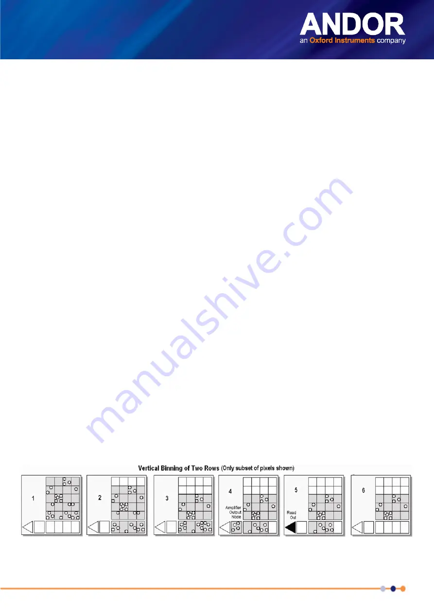
In Vertical Binning, charge from two or more rows of the CCD-chip is moved down into the shift register before the
charge is read out. The number of rows shifted depends on the binning pattern you have selected. Thus, for each
column of the CCD-chip, charge from two or more vertical elements is ‘summed’ into the corresponding element of the
shift register. The charge from each of the pixels in the shift register is then shifted horizontally to the output node of the
amplifier and read out.
Variants of Vertical Binning are used to affect a variety of binning patterns and they are as follows:
•
Single-Track
: charge is vertically binned and read out from a number of complete, adjacent rows of pixels on
the CCD-chip. The rows form a single track across the full width of the CCD-chip. A value is taken for each
column in the track.
•
Multi-Track
: Multi-Track mode differs from Single-Track in that you may now define two or more tracks from
which to read out charge. In processing terms, each track is treated as in Single-Track above.
•
Full Vertical Binning (FVB
): charge from each complete column of pixels on the CCD is moved down and
summed into the shift register and the charge is then shifted horizontally one pixel at a time from the shift
register into the output node - in effect a value is read out for each complete column of the CCD-chip.
The example below illustrates readout of data from adjacent tracks, each track comprising two binned rows of the
CCD-chip.


