MST Construction Manual – Issue 1
Page 7
A link coupled winding provides a low impedance output for the pre-driver built around
transistor Q9. The collector load is another IF transformer (T8) and resonated to the transmit
frequency in the same way as T7. In practice the two transformers form a 2 pole band pass filter
and adjusted to give the desired passband.
3.3
P
OWER AMPLIFIER
Transmit signal from the pre-driver is applied to the driver stage built around transistor Q6. A
BD139 works well here when biased with about 60mA of collector current. The design is well
proven using both shunt and series feedback to provide low input and output impedance and
good stable gain on the low HF bands.
The power amplifier is an IRF510 MOSFET and has been used in many designs. It is a good
candidate for the HF bands and easily provides over 5 Watts PEP of power from a 13.8 V drain
supply. The output from the driver is applied across resistor R38 and becomes the AC drive
component for Q7 gate. Zener diode ZD4 and trimpot VR2 provides a stable and variable DC
gate voltage to place Q7 just into conduction for linear service. There is a short ramp up of the
gate voltage when switching to transmit as capacitor C54 charges and is included to provide a
smooth gate voltage transition.
The drain load for Q7 is a broadband transformer T6. The turns ratio is chosen for best match
and to provide maximum output into a 50 ohm load. The waveform from Q7 can be high in
harmonics and so a 5 pole low pass filter is included to reduce the level of harmonic and other
spurious energy to an acceptable level. The values of the low pass filter components are band
dependant.
When the PTT is operated the transmit/receive relay is energized and the filtered transmit
signal is passed to the antenna. When the PTT is not operated the relay switches the antenna
through to the receive circuits. The relay also switches power to the transmit and receive
sections as required.
As a visual indication of power output and modulation, the transmit signal is sampled, rectified
and filtered by R39, D11 and C63. The resultant voltage is buffered by transistor Q8 to drive a
front panel LED via current limiting resistor R41.
The power supply is made available at an auxiliary connector and is intended to power a
companion VFO.
3.4
R
ECEIVE MIXER
Signals from the antenna are applied to a bandpass filter formed with two transformers T2, T3
and capacitors C21, C22 and C23. The antenna is link coupled to T2 while the output is fed from
a tap on the tuned primary winding of T3 to provide proper impedance matching.
The mixer U1 is another SA612. The input is protected with a pair of back to back diodes and fed
single ended into pin 1. Pin 2 is grounded to RF by C25. Zener diode ZD2 provides a stabilized
6.8 volt supply. VFO signal is injected into pin 6 at about 300mV pk-pk. The balanced output
which is a difference signal at approximately 10MHz is fed to broadband transformer T4. The
output of T4 is passed to the crystal filter when DC current flows through R19 and into D6.
Summary of Contents for MST400
Page 1: ...MST Construction Manual Issue 1 Page 1 MST CONSTRUCTION MANUAL ...
Page 9: ...MST Construction Manual Issue 1 Page 9 Figure 2 SSB generator ...
Page 10: ...MST Construction Manual Issue 1 Page 10 Figure 3 Transmit mixer ...
Page 11: ...MST Construction Manual Issue 1 Page 11 Figure 4 Power amplifier ...
Page 12: ...MST Construction Manual Issue 1 Page 12 Figure 5 Receive mixer ...
Page 13: ...MST Construction Manual Issue 1 Page 13 Figure 6 Receive audio ...
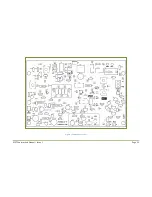
Page 22: ...MST Construction Manual Issue 1 Page 22 Figure 7 Component overlay ...
Page 25: ...MST Construction Manual Issue 1 Page 25 Figure 8 Front panel drilling guide ...


