


2SC3757
2
SJC00136CED
h
FE
I
C
f
T
I
E
C
ob
V
CB
I
C
V
CE
V
CE(sat)
I
C
V
BE(sat)
I
C
220
Ω
0.1
µ
F
50
Ω
V
CC
=
3 V
V
OUT
3.3 k
Ω
50
Ω
V
IN
=
10 V
3.3 k
Ω
V
BB
= −
3 V
V
IN
V
OUT
t
on
90%
10%
90%
10%
t
off
(Waveform at A)
V
IN
V
OUT
10%
10%
t
stg
910
Ω
0.1
µ
F
0.1
µ
F
A
90
Ω
V
CC
=
10 V
V
OUT
500
Ω
50
Ω
V
IN
=
10 V
500
Ω
1 k
Ω
V
BB
=
2 V
t
on
, t
off
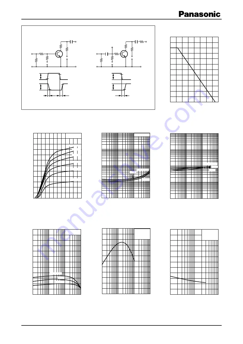
test circuit
t
stg
test circuit
Switching time measurement circuit
P
C
T
a
0
160
40
120
80
0
240
200
160
120
80
40
Collector power dissipation P
C
(mW
)
Ambient temperature T
a
(
°
C)
0
1.2
1.0
0.8
0.2
0.6
0.4
0
120
100
80
60
40
20
T
a
=
25
°
C
2.5 mA
2.0 mA
1.5 mA
1.0 mA
0.5 mA
I
B
=
3.0 mA
Collector current I
C
(mA
)
Collector-emitter voltage V
CE
(V)
0.1
1
10
100
0.01
0.1
1
10
100
I
C
/ I
B
=
10
T
a
=
75
°
C
25
°
C
−
25
°
C
Collector-emitter saturation voltage V
CE(sat)
(V
)
Collector current I
C
(mA)
1
10
100
1 000
0.01
0.1
1
10
100
T
a
=
−
25
°
C
25
°
C
75
°
C
Base-emitter saturation voltage V
BE(sat)
(V
)
Collector current I
C
(mA)
0.1
1
10
100
0
600
500
400
300
200
100
V
CE
=
1 V
T
a
=
75
°
C
25
°
C
−
25
°
C
Forward current transfer ratio h
FE
Collector current I
C
(mA)
−
1
−
10
−
100
−
1 000
0
600
500
400
300
200
100
V
CB
=
10 V
T
a
=
25
°
C
Transition frequency f
T
(MHz
)
Emitter current I
E
(mA)
1
10
100
0
6
5
4
3
2
1
I
E
=
0
f
=
1 MHz
T
a
=
25
°
C
Collector-base voltage V
CB
(V)
Collector output capacitance
(Common base, input open circuited)
C
ob
(pF)
This product complies with the RoHS Directive (EU 2002/95/EC).


