background image


Operation manual for Narrow-pitch connectors A35UH


Panasonic Corporation
industrial.panasonic.com/ac/e/ 


©

 Panasonic Corporation 2017 

ACCTF32E 201704 

- 14 -


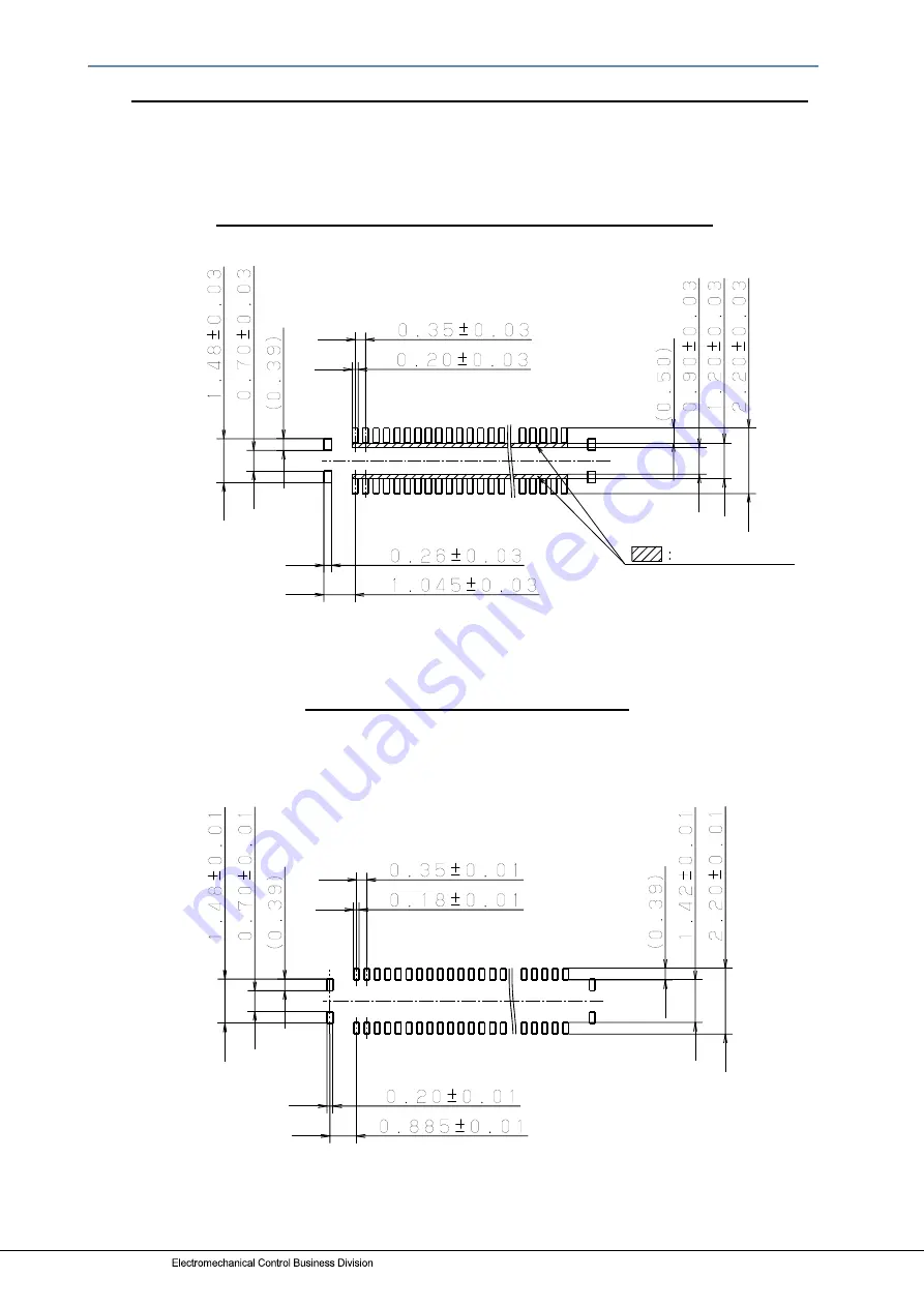
Recommended specifications for PC-board and metal mask opening area 

Applicable product:A35US narrow-pitch connector header 

Mated height

0.6mm


Recommended PC-board pattern (Mount-pad layout)


Recommended metal mask pattern


When the metal mask thickness is 100 

µ

m


(Terminal section opening area: 70%)


(Metal section opening area: 77%) 


 Insulation area


Summary of Contents for A35UH

Page 1: ...ACCTF32E 2017 04 industrial panasonic com ac e A35UH Stacking Connectors for high current Operation manual ...

Page 2: ... e Panasonic Corporation 2017 ACCTF32E 201704 1 Contents 01 Introduction 2 02 Precautions for product design 3 03 Precautions for mounting and reflow soldering 15 04 Precautions for mating and unmating 25 Points which particularly need to be confirmed before designing products are bold and underlined ...

Page 3: ...ion A35UH A35S Space saving Excellent Width 2 2mm Very good Width 2 5mm Low profaile Excellent Mated height 0 6mm Very good Mated height 0 8mm High current Excellent With power terminal Max 10A at total Good No power terminal Max 4A at total Wiring underneath Good Exposed metal part on the rear face Exposed metal part Good Exposed metal part on the rear face Exposed metal part Contact reliability ...

Page 4: ...he connector in the mounting process Design multi pin connector layouts that do not require a swinging movement during pickup and mounting In many cases deviation of the connector mounting position is caused by the inertia of the swinging movement of the mounter A layout that does not require swinging is thus required Example of a connector layout requiring a swinging movement in the mounting proc...

Page 5: ...or may damage it Pay attention to the following points Cushioning material Casing Sub board flexible board Connector Reinforcing plate Motherboard When an impact such as dropping as shown in the drawing is applied 1 If both boards are not sufficiently fixed the connector will be damaged due to the impact applied to the connector 2 In particular if there is no gap between the casing and sub board A...

Page 6: ...cilitate the mating of connectors we recommend that you pay attention to the following points when designing the motherboard Provide a reference mark Design a layout that allows easy checking of the connector mating condition Examples of reference mark Flexible board Reinforcing plate Motherboard Provide a reference mark Silk printing Pattern copper foil ...

Page 7: ...ent When designing in order to prevent an excessive temperature rise make sure to design a foot pattern for the power terminal 3 Pay attention to the following points when providing a through hole by extending the foot pattern If a through hole is created simply by extending the foot pattern by the same width solder is absorbed into the through hole during the reflow process which may cause defect...

Page 8: ...ve the minimum area on the premise that the reflow soldering process is used For manual soldering or for ensuring solder reworkability make a longer pattern at the terminal tip 6 When it is needed to provide pattern wiring and through hole underneath the socket it is possible to use it by designing the pattern as shown below in case insulation underneath the socket is not assured Secure space for ...

Page 9: ...ic com ac e Panasonic Corporation 2017 ACCTF32E 201704 8 7 Resist between pins When it is needed to provide resist between the pins there is a way to adopt the overresist method as below If the resist is out of alignment the pattern width 0 20mm would not change Copper foil Overresist Resist ...

Page 10: ...inEtsu Polymer In case of a one sided FPC board warpage is more likely to occur if a pattern is laid in a line or if the copper foil is applied over the entire FPC board for noise prevention purposes Since the FPC is soft it is difficult to keep it flat Typical transfer jigs for the board mounting process Magic resin Daisho Denshi Keiju board Mitsubishi Resin Assist carrier ShinEtsu Polymer To kee...

Page 11: ...out 30 μm including the adhesive If the thickness exceeds 30 μm design the board so as to remove the coverlay under the connector 3 This connector is often used for connecting the motherboard and FPC board In this case if the FPC board is too short a load that causes deviation will be applied to the connector Make sure to create a design that provides some allowance in the FPC board Connector term...

Page 12: ...y occur depending on the direction the reinforcing plate on material was cut Accordingly make sure to indicate the direction of the material Rolled sheets generate warpage depending on material direction so therefore make sure to warpage reduction into consideration 4 For using an ultra thin reinforcing plate for slimming a product one way is to use metals such as stainless steel for the reinforci...

Page 13: ... Make sure to adjust the amount of solder applied after checking the finish quality in a test run 2 Compared with natural air reflow soldering N2 reflow soldering can reduce oxidization of the melted solder surface This significantly improves the solder wettability Therefore make sure to apply an appropriate amount of solder 3 Do not apply an excessive amount of solder otherwise solder or flux may...

Page 14: ...cations for PC board and metal mask opening area When designing please verify with the product specification sheets Applicable product A35US narrow pitch connector socket Mated height 0 6mm Recommended PC board pattern Mount pad layout Recommended metal mask pattern When the metal mask thickness is 100 µm Terminal section opening area 70 Metal section opening area 46 ...

Page 15: ...704 14 Recommended specifications for PC board and metal mask opening area Applicable product A35US narrow pitch connector header Mated height 0 6mm Recommended PC board pattern Mount pad layout Recommended metal mask pattern When the metal mask thickness is 100 µm Terminal section opening area 70 Metal section opening area 77 Insulation area ...

Page 16: ...cover tape in dry condition Recommended humidity is from 40 RH to 60 RH and please remove static electricity by ionizer in manufacturing process 03 2 Points to consider when selecting a pickup nozzle for mounting Select a pickup nozzle with a suction area that demonstrates a theoretical lifting force at least 10 times greater than the connector weight Theoretical lifting force g Vacuum pressure mm...

Page 17: ...tion 2017 ACCTF32E 201704 16 Examples of suction nozzle shape Connector weight socket Number of pins 10 20 30 40 50 60 70 Weight 0 008 0 011 0 014 0 017 0 020 0 023 0 026 Elongated hole Circular hole Available for less than 50 pins and except for the case of connector turning around when mounted Unit g Mated height 0 6mm ...

Page 18: ... area on the header is 0 8 mm in the shorter direction If it is difficult to reliably insert the nozzle to the connector bottom face of 0 8 mm widthwise the header can be picked up by converting the entire top face of the connector as shown below 2 Dimension of the socket Header Suction area Terminal coplanarity Unit mm Post and soldering terminal Cross section view Mated height 0 6mm ...

Page 19: ... 0 6 30 6 5 1 8 4 5 0 6 40 8 0 1 8 6 0 0 6 50 10 0 1 8 8 0 0 6 60 11 5 1 8 9 5 0 6 70 13 5 1 8 11 5 0 6 Connector weight header Number of pins 10 20 30 40 50 60 70 Weight 0 003 0 004 0 006 0 007 0 009 0 010 0 012 Elongated hole Circular hole Available for less than 50 pins and except for the case of connector turning around when mounted Unit mm It is available to suck the connector s whole top sur...

Page 20: ...plied or the wicking phenomenon may have occurred Check the amount of solder applied the position and the temperature profile at the mounted connector position In particular be careful not to apply excessive solder when the N2 reflow furnace is used 4 Extending the screen pattern outward and providing a solder application position on the outer side can help secure a large front fillet 5 In the ref...

Page 21: ... 2 During solder rework solder is supplied at and the soldering iron is applied to the tip of each pattern Make sure that solder and the soldering iron do not contact the terminal 3 When carrying out manual soldering or rework avoid using flux if possible in order to prevent it from rising to the contact section For details see the next page 4 When using flux apply as little as possible to the tip...

Page 22: ...unt of flux e g BON 102F Japan Bonkote 2 Selection of soldering iron For narrow pitch connectors with a 0 35 mm pitch we recommend An iron tip with a retractable knife shape Ex Japan Bonkote With a temperature sensor on the iron tip Temperature controllable iron tip It is also necessary to check that there are no differences between the indicated temperature and the actual temperature of the iron ...

Page 23: ...on the foot pattern along the terminals without touching them Apply the soldering iron to the foot pattern to heat it Complete soldering in 1 or 2 seconds Connector s resistance to soldering heat 300 C 5 sec max 350 C 3 sec max Thin wire solder with a diameter of 0 3 0 4 mm is recommended Final soldering is recommended after provisionally soldering the terminals at both ends Note that when the sol...

Page 24: ...uct 1 In order to keep the solvent purity and to enhance cleaning prepare equipments such as boil ultrasonic cleaning with cold solvent and vapor washing 2 Keep the cleaning solvent clean and prevent the connector contacts from contamination 3 Some cleaning solvents are strong and they may dissolve the molded part and characters so pure water passed liquid solvent is recommended 4 When cleaning by...

Page 25: ...ning frequency of the mask Considering solder particle diameter and running we recommend the setup as below Solder Cleaning frequency 21 powder Approx third consecutive cleanings 32 powder Max tenth consecutive cleanings 2 Mask opening width Considering solder particle diameter and pattern width we recommend the setup as below Suitable mask opening width for pattern width 0 20mm 3 Pealing force Pr...

Page 26: ...ound will indicate that the simple locking sections are completely mated 4 After completing the mating process check that the clearance between the FPC board and the motherboard is visibly even in both the X and Y directions If the space is not even mating may not be completed Unmate the connectors once check that there is no damage and press them in again 5 In cases when the reinforcing plate is ...

Page 27: ...unmating 1 Hold the reinforcing plate at unmating the connector 2 Lift straight up to unmate 3 If the method of unmating described above is not feasible due to a lack of space around the connector please lift around one of the shorter sides of the connector to unmate it Please avoid completely lifting from the other longer side to unmate which risks damaging the connector Lift up ...

Page 28: ...CTF32E 201704 27 04 3 Proposal on unmating jig Please use the unmating jig if lifting from the other longer side to unmate How to unmate Hook the unmating jig onto one of the shorter side faces of the connector Lift up the jig to unmate one side Remove entirely by hand Detailed drawing of the unmating jig edge General tolerance 0 1 ...

Page 29: ...manual for Narrow pitch connectors A35UH Panasonic Corporation industrial panasonic com ac e Panasonic Corporation 2017 ACCTF32E 201704 28 Amendment history Manual No Date Changes ACCTF32E April 2017 Preliminary ...

Page 30: ...ACCTF32E 201704 2017 ...

Reviews: