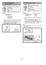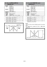
ELE-4
1-7. R, G, B SUB Adjustment
BOARD
PRE AMP
TP
TP102: R
TP302: B
TP202: G
ADJUST
Service Menu
F NUMBER
-----
MODE
-----
CHART
Gray Scale Chart
M. EQ
WFM
SPEC.
As shown below
< Switch Setting >
AUTO W/B BAL
: AWB, ABB
AWB
: A
OUTPUT
: CAM ON
< Menu >
*** CAM DESIGN MENU ***
<VDRIVE 1>
⇒
LIST REG SET1
⇒
R SUB
⇒
ADD _H
⇒
G SUB
ADD_L
⇒
B SUB
WRITE
< Adjustment of Rch, Gch >
1. Adjust iris so that the Gch signal level of SDI OUT
is 70%, and execute the AWB
⇒
ABB.
2. Adjust iris again following above item 1 and
execute the AWB.
3. Aim at the 500 W halogen light and set the zoom
position so that the halogen light size is
approximately 1/10 at the vertical direction of the
monitor.
4. Turn the electric shutter on, and set the shutter
speed to 1/2000.
5. Set the Iris to open. And then confirm the smear
condition.
If the color smear appears, adjust R SUB and G
SUB until the color smear disappears.
6. Set the electric shutter to off and aim at the 2000 lx
grayscale chart at F11-1/2 iris position.
7. Adjust the "VAR" knob on the oscilloscope so that
the level of the signal at the TP102 is 1 scale of
the oscilloscope.
8. Set the Iris to open, and confirm the waveform
level is more than 5 scales. If it is more than 5.5
scales, adjust R SUB on the menu so that the
waveform level is 5.5 scales.
9. Perform the same adjustment from item 6 to 8 for
G channel by TP202/G SUB (menu).
< Adjustment of Bch >
1. Set the OUT PUT SW to CAM OFF.
2. Set the iris to F8-1/4.
3. Adjust the "VAR" knob on the oscilloscope so that
the level of the signal at the TP302 is 0.5 scale of
the oscilloscope.
4. Aim at the halogen lamp directly. (Adjust the zoom
lens so that the illumination of the lamp to fall to
the whole screen.)
5. Set the iris to OPEN.
6. Adjust B SUB so that the peak level of the signal is
6 scales of the oscilloscope.
< Save the Adjustment Value >
To complete this adjustment, "Setting Value Saving" by
the menu is necessary. Execute it according to the
following procedure.
1. set the menu item as shown below, and restart
(OFF
⇒
ON) the unit.
*** CAM DESIGN MENU ***
<LSI REG SET1>
⇒
ADR_H
: FF
⇒
ADR_L
: 08
⇒
WRITE
: OFF
⇒
ON
<Save the Adjustment Value for High Gain>
1. Set the gain switch to "H" (+12 dB)
2. Set the value for SUB as follows.
*** CAM DESIGN MENU ***
<L DRIVE 1>
⇒
R SUB
: A0
⇒
G SUB
: A0
⇒
B SUB
: B0
3. Input as follows.
*** CAM DESIGN MENU ***
<LSI REG SET1>
⇒
ADR_H
: FF
⇒
ADR_L
: 09
⇒
WRITE
: OFF
⇒
ON
4. Set the Power switch to OFF and ON again.
IRIS = F11-1/2
IRIS = OPEN
A
B
0.5 Scales
6 Scales
PRE AMP Board : TP303 (Bch)
Summary of Contents for AJ-HDC27VP
Page 3: ... 3 ...
Page 4: ... 4 ...
Page 6: ... 6 ...
Page 7: ...Printed in Japan FCD0108NCKK71 ...
Page 136: ...ELE 25 9 TP VR and SW Location AUDIO LCD P C BOARD VEP84331B COMPONENT SIDE FOIL SIDE ...
Page 137: ...ELE 26 VIDEO OUT P C BOARD VEP23500B VTR SYSCON P C BOARD VEP86303C COMPONENT SIDE FOIL SIDE ...
Page 138: ...ELE 27 SERVO P C BOARD VEP82224B COMPONENT SIDE FOIL SIDE ...
Page 139: ...ELE 28 VIDEO MAIN P C BOARD VEP83462C COMPONENT SIDE FOIL SIDE ...
Page 140: ...ELE 29 FOIL SIDE DSP MAIN P C BOARD VEP23530B COMPONENT SIDE ...
Page 141: ...ELE 30 VTR MOTHER P C BOARD VEP80B10A RF EQ P C BOARD VEP87104B COMPONENT SIDE COMPONENT SIDE ...
Page 151: ...HEAD BUFFER BLOCK DIAGRAM BLK 6 ...
Page 152: ...BLK 7 RF EQ BLOCK DIAGRAM ...
Page 153: ...HD SDI TX VIDEO MAIN BLOCK DIAGRAM BLK 8 DSP MAIN DSP MAIN DSP MAIN DSP MAIN HD SDI TX ...
Page 155: ...SERVO BLOCK DIAGRAM BLK 10 ...
Page 157: ...VTR SYSCON SD CARD BLOCK DIAGRAM BLK 12 Q1 SD CARD CKK USED USED ...
Page 158: ...POWER MAIN SUB BLOCK DIAGRAM BLK 13 ...
Page 323: ...PRT 2 MECHANICAL CHASSIS ASSEMBLY 1 ...
Page 325: ...PRT 4 MECHANICAL CHASSIS ASSEMBLY 2 ...
Page 327: ...PRT 6 CHASSIS FRAME ASSEMBLY 1 ...
Page 329: ...PRT 8 CHASSIS FRAME ASSEMBLY 2 ...
Page 331: ...PRT 10 CHASSIS FRAME ASSEMBLY 3 ...
Page 333: ...PRT 12 CASSETTE COMPARTMENT ASSEMBLY ...
Page 335: ...PRT 14 PACKING PARTS ASSEMBLY ...
Page 387: ...HEAD BUFFER BLOCK DIAGRAM BLK 6 ...
Page 388: ...BLK 7 RF EQ BLOCK DIAGRAM ...
Page 389: ...HD SDI TX VIDEO MAIN BLOCK DIAGRAM BLK 8 DSP MAIN DSP MAIN DSP MAIN DSP MAIN HD SDI TX ...
Page 391: ...SERVO BLOCK DIAGRAM BLK 10 ...
Page 393: ...VTR SYSCON SD CARD BLOCK DIAGRAM BLK 12 Q1 SD CARD CKK USED USED ...
Page 394: ...POWER MAIN SUB BLOCK DIAGRAM BLK 13 ...
Page 399: ...CBA 5 FOIL SIDE CCD SENSOR P C BOARD VEP20854A FOIL SIDE IC101 E1 IC201 C1 IC301 A1 ...
Page 499: ...ELE 25 9 TP VR and SW Location AUDIO LCD P C BOARD VEP84331B COMPONENT SIDE FOIL SIDE ...
Page 500: ...ELE 26 VIDEO OUT P C BOARD VEP23500B VTR SYSCON P C BOARD VEP86303C COMPONENT SIDE FOIL SIDE ...
Page 501: ...ELE 27 SERVO P C BOARD VEP82224B COMPONENT SIDE FOIL SIDE ...
Page 502: ...ELE 28 VIDEO MAIN P C BOARD VEP83462C COMPONENT SIDE FOIL SIDE ...
Page 503: ...ELE 29 FOIL SIDE DSP MAIN P C BOARD VEP23530B COMPONENT SIDE ...
Page 504: ...ELE 30 VTR MOTHER P C BOARD VEP80B10A RF EQ P C BOARD VEP87104B COMPONENT SIDE COMPONENT SIDE ...
Page 554: ...PRT 2 MECHANICAL CHASSIS ASSEMBLY 1 ...
Page 556: ...PRT 4 MECHANICAL CHASSIS ASSEMBLY 2 ...
Page 558: ...PRT 6 CHASSIS FRAME ASSEMBLY 1 ...
Page 560: ...PRT 8 CHASSIS FRAME ASSEMBLY 2 ...
Page 562: ...PRT 10 CHASSIS FRAME ASSEMBLY 3 ...
Page 564: ...PRT 12 CASSETTE COMPARTMENT ASSEMBLY ...
Page 566: ...PRT 14 PACKING PARTS ASSEMBLY ...


