ELE-1
< CAMERA >
1. OPTICAL UNIT
1-1. Initial Setting
Unless otherwise specified, implement the adjustment
of the optical unit by the following setting.
< Lighting >
For the lighting source, use the halogen lamp of 3200K,
500W and set it to get 2000LUX evenly on the surface
of object.
< Front switch Setting >
AUTO W/B BAL
:
−
GAIN
: L
AWB
: PRST (PRESET)
OUTPUT
: CAM OFF
SHUTTER
: OFF
USER SW 1
: OFF
< Camera Setting >
Lens Extender
: OFF
CC Filter
: 3200K (B)
ND Filter
: CLEAR (1)
< MENU Setting >
*** CAM MAIN MENU4 ***
<BLACK SHADING>
⇒
CORRECT (DIG) “ON
→
OFF”
<WHITE SHADING>
⇒
CORRECT “ON
→
OFF”
*** CAM MAIN MENU2 ***
<RFAME MODE>
⇒
FRAME RATE : 60
< Save the Adjustment Value >
Depending on the adjustment item, it is necessary to
save the data in the flash memory on the CAM SYS
P.C.Board after adjustment.
For saving each adjustment data, follow the instruction
of each adjustment item.
< Menu >
Follow the saving data item.
*** CAM DESIGN MENU ***
<VDRIVE 1>
⇒
R, G, B - SUB
⇒
R, G, B - RESET DC
⇒
H1 DC
How to save.
<LSI REG SE T1>
⇒
ADR_H : “FF”(Input)
⇒
ADD_L : “01” (Input)
⇒
WRITE : "OFF"
!
“ON”
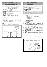
1-2. R, G, B RESET DC Adjustment
BOARD
-----
TP
SDI OUT (G,B,R) 75ohm termination
ADJUST
Service Menu
F NUMBER
F5.6
MODE
-----
CHART
Immega Cycle Chart (For HD)
M. EQ
WFM
SPEC.
At a level just below onset of white
streaking (Waveform Distortion) + 20
(MENU : HEX).
< Camera Setting >
ND Filter
: 1/16 ND (3)
< Menu >
*** CAM DESIGN MENU ***
<VDRIVE 1>
⇒
R RESET DC
⇒
G RESET DC
⇒
B RESET DC
⇒
H1 DC
1. Aim at the immega cycle chart to be full picture of
the monitor.
2. Set the WFM mode to be able to observe R, G, B
signal.
3. Adjusts the each RESET DC so that the value for
each color signal are within the specification.
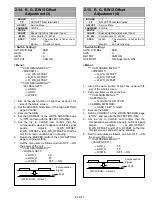
Notes:
1. Initial value of MENU must be "80" and then set to
a value where the signal becomes no distortion.
2. At the end of the adjustment, set ND filter to "1".
Example: If distortion
disappears with
MENU at "7A",
adjustment value is
"9A", if "83", "A3".
Distortion
Summary of Contents for AJ-HDC27VP
Page 3: ... 3 ...
Page 4: ... 4 ...
Page 6: ... 6 ...
Page 7: ...Printed in Japan FCD0108NCKK71 ...
Page 136: ...ELE 25 9 TP VR and SW Location AUDIO LCD P C BOARD VEP84331B COMPONENT SIDE FOIL SIDE ...
Page 137: ...ELE 26 VIDEO OUT P C BOARD VEP23500B VTR SYSCON P C BOARD VEP86303C COMPONENT SIDE FOIL SIDE ...
Page 138: ...ELE 27 SERVO P C BOARD VEP82224B COMPONENT SIDE FOIL SIDE ...
Page 139: ...ELE 28 VIDEO MAIN P C BOARD VEP83462C COMPONENT SIDE FOIL SIDE ...
Page 140: ...ELE 29 FOIL SIDE DSP MAIN P C BOARD VEP23530B COMPONENT SIDE ...
Page 141: ...ELE 30 VTR MOTHER P C BOARD VEP80B10A RF EQ P C BOARD VEP87104B COMPONENT SIDE COMPONENT SIDE ...
Page 151: ...HEAD BUFFER BLOCK DIAGRAM BLK 6 ...
Page 152: ...BLK 7 RF EQ BLOCK DIAGRAM ...
Page 153: ...HD SDI TX VIDEO MAIN BLOCK DIAGRAM BLK 8 DSP MAIN DSP MAIN DSP MAIN DSP MAIN HD SDI TX ...
Page 155: ...SERVO BLOCK DIAGRAM BLK 10 ...
Page 157: ...VTR SYSCON SD CARD BLOCK DIAGRAM BLK 12 Q1 SD CARD CKK USED USED ...
Page 158: ...POWER MAIN SUB BLOCK DIAGRAM BLK 13 ...
Page 323: ...PRT 2 MECHANICAL CHASSIS ASSEMBLY 1 ...
Page 325: ...PRT 4 MECHANICAL CHASSIS ASSEMBLY 2 ...
Page 327: ...PRT 6 CHASSIS FRAME ASSEMBLY 1 ...
Page 329: ...PRT 8 CHASSIS FRAME ASSEMBLY 2 ...
Page 331: ...PRT 10 CHASSIS FRAME ASSEMBLY 3 ...
Page 333: ...PRT 12 CASSETTE COMPARTMENT ASSEMBLY ...
Page 335: ...PRT 14 PACKING PARTS ASSEMBLY ...
Page 387: ...HEAD BUFFER BLOCK DIAGRAM BLK 6 ...
Page 388: ...BLK 7 RF EQ BLOCK DIAGRAM ...
Page 389: ...HD SDI TX VIDEO MAIN BLOCK DIAGRAM BLK 8 DSP MAIN DSP MAIN DSP MAIN DSP MAIN HD SDI TX ...
Page 391: ...SERVO BLOCK DIAGRAM BLK 10 ...
Page 393: ...VTR SYSCON SD CARD BLOCK DIAGRAM BLK 12 Q1 SD CARD CKK USED USED ...
Page 394: ...POWER MAIN SUB BLOCK DIAGRAM BLK 13 ...
Page 399: ...CBA 5 FOIL SIDE CCD SENSOR P C BOARD VEP20854A FOIL SIDE IC101 E1 IC201 C1 IC301 A1 ...
Page 499: ...ELE 25 9 TP VR and SW Location AUDIO LCD P C BOARD VEP84331B COMPONENT SIDE FOIL SIDE ...
Page 500: ...ELE 26 VIDEO OUT P C BOARD VEP23500B VTR SYSCON P C BOARD VEP86303C COMPONENT SIDE FOIL SIDE ...
Page 501: ...ELE 27 SERVO P C BOARD VEP82224B COMPONENT SIDE FOIL SIDE ...
Page 502: ...ELE 28 VIDEO MAIN P C BOARD VEP83462C COMPONENT SIDE FOIL SIDE ...
Page 503: ...ELE 29 FOIL SIDE DSP MAIN P C BOARD VEP23530B COMPONENT SIDE ...
Page 504: ...ELE 30 VTR MOTHER P C BOARD VEP80B10A RF EQ P C BOARD VEP87104B COMPONENT SIDE COMPONENT SIDE ...
Page 554: ...PRT 2 MECHANICAL CHASSIS ASSEMBLY 1 ...
Page 556: ...PRT 4 MECHANICAL CHASSIS ASSEMBLY 2 ...
Page 558: ...PRT 6 CHASSIS FRAME ASSEMBLY 1 ...
Page 560: ...PRT 8 CHASSIS FRAME ASSEMBLY 2 ...
Page 562: ...PRT 10 CHASSIS FRAME ASSEMBLY 3 ...
Page 564: ...PRT 12 CASSETTE COMPARTMENT ASSEMBLY ...
Page 566: ...PRT 14 PACKING PARTS ASSEMBLY ...


