background image

MECH-25

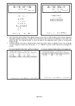
6.  Next, select the Serial number of the Alignment tape on the screen. If LISTA software does not have alignment

tape data registered, data entry is needed. Press the ESC key, then main menu is displayed on the screen. And
select the item “<4>  Alignment Tape” for entry the data on the attachment sheet, which is enclosed with
alignment tape.

7.  If LISTA software has data of alignment tape, select the serial number of Alignment tape, then message

“ok?(y/n)” appears on the screen. And press “ Y ” or “ ENTER ” key, then LISTA main menu is displayed on
screen.

<< In case, Alignm ent Tape data is registered already >>

<< In case,  Alignm ent Tape data is not registered>>

Summary of Contents for AJ-HDC27VP

Page 1: ...on is a violation of law ORDER NO BSD0108M017 D26 AJ HDC27VP Sec 1 Service Information Sec 2 Disassembly Procedures Sec 3 Mechanical Adjustment Sec 4 Electrical Adjustment Sec 5 Block Diagrams Sec 6 Schematic Diagrams Sec 7 Circuit Board Diagrams Sec 8 Exploded Views Replacement Parts List Camera VTR ...

Page 2: ...gs or cautions to advise non technical individuals of potential dangers in attempting to service a product Products powered by electricity should be serviced or repaired only by experienced professional technicians Any attempt to service or repair the product or products dealt with in this service information by anyone else could result in serious injury or death ...

Page 3: ... 3 ...

Page 4: ... 4 ...

Page 5: ...iately before handling any semiconductor component or semiconductor equipped assembly drain off any electrostatic charge on your body by touching a known earth ground Alternatively obtain and wear a commercially available discharging wrist trap device which should be removed for potential shock reasons prior to applying power to the unit under test 2 After removing an electrical assembly equipped ...

Page 6: ... 6 ...

Page 7: ...Printed in Japan FCD0108NCKK71 ...

Page 8: ...the ENG SECURITY INF 13 8 5 Setting Menu Configurations INF 14 9 Service Menu Item Contents INF 17 9 1 CAM SERVICE MENU INF 17 9 2 CAM DESIGN MENU INF 18 9 3 VTR SERVICE 1 3 INF 20 9 4 VTR SERVICE 2 3 INF 21 9 5 VTR SERVICE 3 3 INF 21 9 6 VTR DESIGN MENU INF 21 9 7 TEST MODE INF 22 9 8 ERROR LOG INF 22 10 Adjustment after Optical Unit Replacement INF 23 10 1 Input the Adjustment Data INF 23 10 2 E...

Page 9: ...ion Method INF 38 17 1 Preparation INF 38 17 2 Connection INF 38 17 3 Compensation flow INF 39 17 4 Compensation Procedures INF 40 17 5 Remarks INF 44 17 6 Trouble Shooting INF 45 17 7 FAQ Frequently Asked Question INF 45 ...

Page 10: ...2 L Cassette 29 VFM3582KL Alignment Tape No 3 L Cassette 30 AJ CL12P Cleaning Tape SALES Route 31 VFK1481B LISTA Software 32 VFK1186 LISTA Cable 33 VFK0369 Tweezers 34 VFK0371 Radio Prier 35 VFK0372 Cutter Prier 36 VFK0337 Phillips Driver 37 VFK0338 Phillips Driver 38 VFK1369 Tape Sensor Adjustment Cassette 39 VFK0906 Lubrication Oil 40 VFK1642 Gray Scale Chart Reflection type 16 9 41 VFK1643 Reso...

Page 11: ...155 REV Position Tool Silver 10 VFK1156 PLAY Position Tool Black 11 VFK1208 Neutral Position Tool Black with Hole 12 VFK1150 Nut Driver 5 5mm 13 VFK1151 Nut Driver 2 5mm VFK1188A 30mN 14 Dial Tension Gauge VFK0948 15 Check Light VFK0749 16 Froiral Grease for Plastic MOR265 17 Morlytone Grease for Metallic VFK1146 18 VFK1147 19 Phillips Driver Fine VFK1148 1 5mm 20 VFK1178 0 89mm 21 VFK1179 0 71mm ...

Page 12: ...rier VFK0337 Phillips Driver VFK0338 Phillips Driver VFK1369 Tape Sensor Adjustment Cassette VFK0906 Lubrication Oil 40 41 42 VFK1643 Resolution Chart 16 9 Reflection type VFK1642 Gray Scale Chart 16 9 Reflection Type VFK1644 Immega Chart For HD Transpalency Type 43 VFK1194 Extender Board VFK1600 44 VFK1602 46 VFK1604 47 VFK1605 48 VFK1606 49 VFK1607 50 VFK1607 51 Wire Harness VFK1601 45 VFK1609 5...

Page 13: ...hen disconnect connectors P100 P300 2 Connection of VFK1611 1 Connect Connector P5 on VFK1611 to Connector P4 on CAMERA MOTHER P C Board 3 Connection of DSP3 P C Board 1 Connect connector P500 on DSP3 P C Board to connector P8 on VFK1611 4 Connection of VFK1604 1 Connect following connectors between DSP3 P C Board and CAMERA MOTHER P C Board by VFK1604 2x DSP3 P C Board CAMERA MOTHER P C Board P30...

Page 14: ...ing 1KHz 20dB Confirmation of the Audio Level 2 1 2 VFM3581KL Time VIDEO PCM CUE min SIGNAL PORPOSE SIGNAL PORPOSE SIGNAL PORPOSE 0 00 ITI Pattern Linearity Adjustment 2 1 3 VFM3582KL Time VIDEO PCM CUE min SIGNAL PORPOSE SIGNAL PORPOSE SIGNAL PORPOSE 0 00 Color Bar 75 with drop out track X Value Adjustment 6KHz 10VU X Value Adjustment 3 List of Recommended Measuring and Instruments MODEL No Examp...

Page 15: ...noid IM 18 Main Cam Gear IM 19 Mechanism Unit IM 20 Cassette Compartment Unit IM Replacement of the mechanism chassis unit is recommended for the 12 000 h maintenance C Perform cleaning R Assembly subject to exchange Y The timing of replacement with Cleaning Arm Unit either 1000 hours or 1 year as timing come earlier G At the time of replacement wipe off the old grease and apply new grease Molyton...

Page 16: ... Cleaning Arm Unit A C Head Loading Motor Pinch Solenoid Capstan Motor Thrust Screw Unit Tape BEG END Detect Sensor Pinch Arm Unit T Reel Motor Unit T Brake Arm Unit L Switch Base Unit T Brake Solenoid S Brake Solenoid T Brake Arm Unit T Reel Motor Unit Tension Sensor Tape End Detect Sensor ...

Page 17: ...eeds to be rotated through about 90 turns after the first turn until the tape is ejected 4 Remove the cassette 5 Return the rubber cap to its original position Notes Do not turn the EMERGENCY screw except in an emergency Do not turn the screw clockwise Stop turning the screw as soon as the tape is ejected Otherwise the mechanism may be damaged After the tape is ejected the cassette holder will not...

Page 18: ...3 A C Head Cleaning Method Weekly Wipe the A C head with a cloth dipped in cleaning liquid Wipe again with a dry cloth 7 4 Pinch Roller and Capstan Shaft Cleaning Method Weekly Wipe the Pinch Roller and Capstan with a cloth dipped in cleaning liquid 7 5 Post Cleaning Method Weekly Wind a cloth on a pick Wipe each posts with that pick Wipe again with a dry cloth For metal posts wipe with a cloth di...

Page 19: ...ENU screen is displayed CAM MAIN MENU1 Press the SHIFT buttons simultaneously and press the MENU button Press the MENU button VTR MAIN MENU Press the JOG dial button CAM MAIN MENU2 CAM MAIN MENU3 CAM MAIN MENU4 Press the JOG dial button Press the JOG dial button Press the JOG dial button Press the MENU button Press the MENU button Press the MENU button CAM SERVICE MENU Press the JOG dial button Pr...

Page 20: ...yed by pressing the JOG Dial button Press the SHIFT RESET buttons simultaneously and press the MENU button CAM MAIN MENU1 Press the MENU button VTR MAIN MENU Press the JOG dial button CAM MAIN MENU2 CAM MAIN MENU3 CAM MAIN MENU4 Press the JOG dial button Press the JOG dial button Press the JOG dial button Press the MENU button Press the MENU button Press the MENU button CAM SERVICE MENU Press the ...

Page 21: ...sidce the title part of the SUB MENU Example Turn the JOG Dial button C A M M AI N M EN U1 ROP MATRIX COLOR CORRECTION1 COLOR CORRECTION2 LOW SETTING MID SETTING HIGH SETTING ADITIONAL DTL1 ADITIONAL DTL2 SKIN TONE DTL KNEE LEVEL GAMMA CAMERASETTING Press the JOG Dial button C A M M AI N M EN U1 ROP MATRIX COLOR CORRECTION1 COLOR CORRECTION2 LOW SETTING MID SETTING HIGH SETTING ADITIONAL DTL1 ADIT...

Page 22: ...tings menu mode and return to the normal operation mode NOTE To exit the camera unit s menu press the MENU button twice When the MENU button is pressed once operation is transferred to the VTR unit s menu 8 4 How to release the ENG SECURITY There is a ENG SECURITY menu in the OPTION screen of the engineer menu When set this item to ON the engineer menu is not displayed When you want to release thi...

Page 23: ...OR GAIN OFFSET LEVEL A OFFSET LEVEL B ENTRY CANCEL DEFECT NO DEFECT SIZE DEFECT COLOR GAIN OFFSET LEVEL A OFFSET LEVEL B CHANGE DELETE ALL DATA CLEAR DETECTION DIGITAL EDIT DELETE SERVICE ADJ R GAMMA SERV G GAMMA SERV B GAMMA SERV DEFECT COMPENSATION COMPENSATION COMP ON GAIN INTERLACE MODE R CH G CH B CH TRIPLE OFFSET CURSOR BOX READ DATA WRITE DATA NG LIST NO SELECT ENTRY CURSOR DISP R W SEL REA...

Page 24: ...0 or B 1 MEMORY SEL ADR H ADR L DATA H DATA L WRITE READ A 0 or B 1 MEMORY SEL ADR H ADR L DATA H DATA L SHAD DA SET KNEE APA SET BSHD_R BSHD_G BSHD_B WSHD_G_SUB WSHD_B WSHD_G WSHD_R IRIS_C THRESH LEVEL SLOPE FREQ GAIN CORING LVL DTL COMP DTL COMP DTL CLIP DTL CLIP KNEE SET ADR DATA WRITE IRIS POS ZOOM POS FOCUS POS LENS EXT CC FILT ND FILT PEAKING FRAME ZEBRA MARK SW GAIN G GAIN B GAIN R CPL G CP...

Page 25: ...J MODE VTR SERVICE MENU VTR SERVICE 1 3 VTR SERVICE 2 3 VTR SERVICE 3 3 VTR D A DATA CONCEAL INNER ECC OUTER ECC VITERBI ADJUST ADDRESS AUDIO PB SEL AUDIO SAVE AUDIO CH7 8 ADJUST DATA BER ADJ BER SPEED CW REC AUTO EQ RDS REC ADJ RDS TYPE SERVO MODE T TORQUE S TORQUE PG SHIFT 100 HSW_A_RIZE HSW_A_FALL HSW_C_RIZE HSW_C_FALL RPL GAIN 100 RPL LIN 100 CTL ADJ X VALUE SET X VALUE 100 TRK VAL 100 SERVO M...

Page 26: ...FF ON Factory Use ENTRY MANUAL H CURSOR COARSE 00 08 03 Coarse Adjustment for Horizontal Cursor Position H CURSOR FINE 00 FF 80 Fine Adjustment for Horizontal Cursor Position V CURSOR COARSE 00 04 02 Coarse Adjustment for Vertical Cursor Position V CURSOR FINE 00 FF 80 Fine Adjustment for Vertical Cursor Position DEFECT SIZE 1 3 1 Sequential Number of blemish DEFECT COLOR Y R G B Y The color which...

Page 27: ...e voltage of CCD VAL VBL 00 FF 40 Transfer Pulse voltage of CCD VBL LG 00 FF 6A Output Amp Voltage of CCD LG HPP 00 FF FF H Transfer Pulse voltage of CCD H 0D 00 FF FF Output Amp Voltage of CCD OG P16V 00 FF FF CCD Drive voltage 16V R_PADC 00 FF A8 Offset Adjustment for Rch Pre Amp G_PADC 00 FF 98 Offset Adjustment for Gh Pre Amp B_PADC 00 FF C7 Offset Adjustment for Bch Pre Amp DA RESET OFF ON OF...

Page 28: ... DATA_L Not Used SHAD DA SET BSHD_R BSHD_G BSHD_B WSHD_G_SUB WSHD_B WSHD_G WSHD_R IRIS_C Factory Use only Fixed at Factory KNEE APA SET TRESH LEVEL SLOPE FREQ GAIN CORING LVL DTL COMP DTL COMP DTL CLIP DTL CLIP KNEE SET Not Used LSIC REGSET ADR Not Used DATA Not Used WRITE Not Used AD READ TEST IRIS POS Lens iris position information ZOOM POS Lens zoom position information FOCUS POS Lens focus pos...

Page 29: ...FILTER POSITION 3 POSITION4 R 127 128 0 R GAIN Adjustment at ND FILTER POSITION 4 POSITION1 B 127 128 0 B GAIN Adjustment at ND FILTER POSITION 4 VTR Section 9 3 VTR SERVICE 1 3 ITEM SETTING RANGE INIT VALUE Backup Backup INH MEANING of SETTING OUTLINE of FUNCTION CONCEAL ON OFF ON NG NG CONCEAL setting INNER ECC ON OFF ON NG NG INNER ECC setting OUTER ECC ON OFF ON NG NG OUTER ECC setting VITERBI...

Page 30: ...tment RPL LIN 100 OFF ON OFF NG NG RPL head LISTA linearity adjustment CTL ADJ OFF ON OFF NG NG CTL Adjust mode setting X VALUE SET OFF ON OFF NG NG X value adjustment X VALUE 100 128 127 0 OK NG Fine adjustment for X value TRK VAL 100 128 127 0 NG NG CTL tracking offset setting SERVO MODE ATF CTL ATF NG NG Servo mode setting 9 5 VTR SERVICE 3 3 ITEM SETTING RANGE INIT VALUE Backup Backup INH MEAN...

Page 31: ...r Cannot delete until execute LOG ALL CLEAR LOG ALL CLEAR OFF ON OFF ON All Clear Finally turn OFF or POWER OFF ERROR CODE E 00 SEQUENCE NO 00 DATE 00 01 01 TIME 12 34 56 OPERATION TIME 000000Hr TAPE TOTAL 120min TAPE REMAIN 90min BATTERY METER 1 F Example a F a indicates the meter number F indicates the blink flash OBJ MODE 00 00 00 00 00 00 00 12 34 56 Indicate the time when OBJ MODE occurred 00...

Page 32: ... Adjustment Data Sheet 8 items CAM DESIGN MENU VDRIVE 1 R SUB R RESET DC G SUB G RESET DC B SUB B RESET DC CAM DESIGN MENU VDRIVE 2 H1 DC VSHIN 3 Input or execute the following setting by menu Memory of Setting Value CAM DESIGN MENU LSI REG SET 1 ADR_H FF input ADR_L 01 input WRITE OFF ON execute 10 2 Electrical Adjustment Execute the Confirmation and Adjustment as following items Refer to Section...

Page 33: ...ay T 59 94Hz E 59 94Hz 50Hz P 50Hz Ver T1 00 01 1 00 Software Version DIAGNOSTIC CAMSOFT IN Ver T1 00 01 1 00 CAMSOFT OUT Ver T1 00 01 1 00 GAMMA GAIN Ver T1 00 01 1 00 GAMMA RAM Ver T1 00 01 1 00 KNEE Ver T1 00 01 1 00 ALC Ver T1 00 01 1 00 PLD Ver T1 00 01 1 00 Flash memory Included IC1 Software Version Flash Memory IC2 Software Version GAMMA Table Software Version Black GAMMA Table Software Ver...

Page 34: ...IGN MENU page Press JOG Dial 3 Select VTR DESIGN MENU item Turn press JOG Dial 4 After the following figure is displayed move to the item to reset VTR DESIGN MENU VTR DESIGN MENU TEST MDOE ERROR LOG VM PLD V0 00 VTR SYSCON V18388a 00 06 13 VTR DESIGN MENU MENU ALL INIT DRUM RUNNING RESET THREADING RESET ...

Page 35: ...age Turn press JOG Dial 3 Confirm BER SPEED setting is SLOW 4 Select BER ADJ by rotating JOG Dial and Select R P head to be confirmed BER ADJ item OFF L1L3 R1R3 L2L4 R2R4 exept OFF 5 The Error rate will be displayed in the Audio meter on the Audio LCD panel 40 dB 30 20 10 0 AUDIO LCD METER Error rate Spec A CH1 CH2 L1 R1 L2 R2 L3 R4 L3 R4 ...

Page 36: ...ng 60dBu 40dBu SW42001 60 REAR CH2 MIC input level setting 60dBu 40dBu SW41002 40 FRONT CH1 MIC input level setting 50dBu 40dBu SW42002 40 FRONT CH2 MIC input level setting 50dBu 40dBu VTR SYSCON 1 OFF FIXED Not used 2 OFF EE ROM write protect allow is ON side SW500 3 4 OFF FIXED Factory use only 1 OFF FIXED Not used 2 OFF EE PROM initialize ROM initialization procedure 1 Turn Off the unit 2 Switc...

Page 37: ...P C BOARD E40 SDI BNC P C BOARD E18 REAR JACK P C BOARD E32 OPERATE P C BOARD E38 BACK TALLY P C BOARD E39 SIDE BNC P C BOARD E30 REAR SW P C BOARD E31 CUE P C BOARD E7 1 DSP MAIN P C BOARD E2 TG P C BOARD E1 PRE AMP P C BOARD E7 2 MEMORY P C BOARD E25 CCD SENSOR P C BOARD E3 DRIVE P C BOARD E34 SD CARD P C BOARD E28 FRONT TOGGLE P C BOARD E29 JOG MENU P C BOARD E33 FRONT MIC P C BOARD E4 PRE PROC...

Page 38: ... Notice Flash memory software versions on each P C Board sometimes need to be upgraded together with PLD version up Before PLD version up confirm the instruction of each vsi file Personal Computer With WINDOWS 95 or 98 15 2 Connection IC100 CAM_SYS P C Board 1 Connect D sub cable between connector CN201 on VFK1590 and PC 2 Connect CPLD Writer cable between connector P201 on VFK1590 and connector P...

Page 39: ...then Programmer 3 On main window Programmer window is displayed select tab Options and then Hardware Setup 4 On Hardware Setup dialog set Hardware Type to ByteBlaster MV 5 On main window select tab File Project and then Name 6 On Dialog of Project Name select the TDF file IC100 or POF file IC321 and then Click OK button ...

Page 40: ... 10 through 16 in this service manual for how to open each menu screen DIAGNOSTIC VTR DESIGN MENU CAMSOFT IN CAMSOFT OUT GAMMA GAIN GAMMA RAM KNEE PLD Ver T1 xx 01 1 xx Ver T1 xx 01 1 xx Ver T1 xx 01 1 xx Ver T1 xx 01 1 xx Ver T1 xx 01 1 xx Ver T1 xx 01 1 xx DESIGN MENU TEST MODE ERROR LOG VM PLD VTR SYSCON V x xx V1 8126a 00 00 00 DIAGNOSTIC page VTR DESIGN page MAX PLUS is registered trademark o...

Page 41: ...able 9pins 9pins Cross type D SUB Version upgrade Software CAM_SYS P C B VTR_SYS P C B SERVO P C B XXXXX BAT come with each Version up data VFK1248E For WINDOWS 95 or 98 type VFK1503 Version up Data VVVSI File Personal Computer With MS DOS Windows95 or Windows 98 MS DOS Windows95 and Windows98 are either registered trademarks of Microsoft corporation in the United States and or other countries Com...

Page 42: ...User data with Multimedia Card See Operating Instructions page numbers 59 63 for Details of Getting the User data 16 2 2 Connection 1 Connect RS 232C Cable between connector P2 on VFK1304A and COM1 port on PC Refer to Figure 16 2 2 Connect Flat cable between connector P1 on VFK1304A and connector P2 on CAM_SYS P C Board and then set SW1 on VFK1304A according to Figure 16 1 3 Set SW201 on CAM_SYS P...

Page 43: ... is completed 5 Set SW201 to OFF side 6 Turn OFF ON the power of camcorder and then confirm software s version NOTE Each software version is indicated on DIAGNOSTIC menu screen CAM MAIN MENU4 page 16 2 4 Restoring User Data 1 Restore the User data with Multimedia card See Operating Instructions page numbers 59 63 for Details of restoring the User data 16 2 5 Trouble Shooting Symptoms Error message...

Page 44: ...ersion Upgrading 1 Copy all files of VFK1248E to arbitrary directory 2 Double click the program file icon VSI2312E EXE 3 When this Software is started a dialog will be opened as shown below 4 Set parameters on Setup Panel window Microcomputer select M32160F4UFP Writing data File data Enter new version up data name XXXX mot with full path You can also use Browse button on the Setup panel to select ...

Page 45: ...emory While processing progress status can be confirmed by means of Process indicator If the Indicator doesn t advance for some reason click Emergency stop C button and then confirm settings 8 When Process bar reaches at 100 position and Waiting to start or Completed indicator is marked Version up is completed then click Exit X button 9 Turn off the power of DC power supply and then set the power ...

Page 46: ... of version up data and SERVO Version upgrade software VFK1503 to the same directory SERVO Version upgrade software VFK1503 fw103u exe SERVO Version upgrade data vsiXXXX obf vsiXXXX bat vsiXXXX ex 5 Type vsixxxx bat and then hit RETURN key 6 Type Y and then hit RETURN key after display message DO YOU CONTINUE Y N 7 Data transfer will be started 8 After data transfer is finished turn off the power ...

Page 47: ...o it is possible to manual compensate too 17 1 Preparation 1 Need about 2 hours aging before start an adjustment 2 Set WHITE BAL SW CC and ND filter wheels as shown below WHITE BAL SW PRST CC FILTER Position B ND FILTER Position No 1 3 Close LENS Iris and then execute ABB by the front switch 17 2 Connection To facilitate blemish compensation s work connect the camcorder and the HD TV monitor throu...

Page 48: ...COMPENSATION menu setting Execute automatic compensation ENTRY AUTO menu Result confirmation at TV monitor Automatic Blemish detection through compensation in whole screen Store result of compensation To built in Memory Only when executed manual adjustment Fine adjustment by cursor manually Only when it cannot compensate completely by automatic compensation ...

Page 49: ...l 4 Set the automatic compensation signal level contrast ratio 1 with PICKUP LEVEL R G or B items The AJ HDC27VP detects blemish which bevel is more than the specified level by this set up ENTRY AUTO PICKUP LEVEL R PICKUP LEVEL G PICKUP LEVEL B START NG LIST NO SELECT ENTRY CURSOR DISP 000 000 000 OFF 000 OFF OFF Figure Ble 2 ENTRY AUTO page 1 contrast ratio blemish signal level patio at the Built...

Page 50: ...enu item s value The number of the points which were detected and compensated as blemish es Display the each color Y shows two or more blemishes were detected at the same position The number of the position because that was which wasn t compensated in compensation inhibition position refer to 17 5 4 Observation environment Measurement part HD SDI OUT connector Circumstance temperature 77 F 25 C GA...

Page 51: ...R G B or Y according to color of blemish If two or more color of blemish appear in the same position select Y ENTRY MANUAL H CURSOR COARSE H CURSOR FINE V CURSOR COARSE V CURSOR FINE DEFECT SIZE DEFECT COLOR GAIN OFFSET LEVEL A OFFSET LEVEL B ENTRY CANCEL 03 80 02 80 3 Y OFF 100 2 100 2 OFF OFF Figure Ble 4 ENTRY MANUAL page 7 Observe TV monitor and then adjust H CURSOR COARSE and FINE item so tha...

Page 52: ...w DEFECT SIZE 3 GAIN OFF 6 Set DEFECT COLOR item to R G B or Y according to color of blemish When two or more color of blemish appear in the same position select Y ENTRY MANUAL H CURSOR COARSE H CURSOR FINE V CURSOR COARSE V CURSOR FINE DEFECT SIZE DEFECT COLOR GAIN OFFSET LEVEL A OFFSET LEVEL B ENTRY CANCEL 03 80 02 80 3 Y OFF 100 100 OFF OFF Figure Ble 5 ENTRY MANUAL page 7 Observe TV monitor an...

Page 53: ...ut blemish compensation 1 Open EDIT DELETE page in CAM SERVICE level 2 Select DEFECT NO to desired position of cursor 3 Change some parameters in EDIT DELETE page DEFECT COLOR DEFECT SIZE etc 4 Set CHANGE item to ON by JOG DIAL operation 5 When CHANGE character appears on the lower right of the screen data change will be completed 6 Close menu screen and then turn off the power of the Unit 17 5 4 ...

Page 54: ...uently Asked Question Question Answer When execute blemish compensation Which should I set to position of GAIN SW on the unit In the AJ HDC27VP GAIN setting while the blemish compensation used by only MENU setup Therefore you don t have to set GAIN SW to some position By setting value of COMP ON GAIN item in the DEFECT COMPENSATION page it is possible to enable compensation in case of level more t...

Page 55: ...art DIS 1 1 1 Removal of the Cassette Cover DIS 1 1 2 Removal of the Left Side Panel DIS 1 1 3 Removal of the Right Side Panel DIS 1 1 4 Removal of the Cassette up Unit DIS 2 1 5 Removal of the Mechanism Unit DIS 2 1 6 Removal of the Cylinder Unit DIS 3 1 7 Removal of the Camera Assembly DIS 4 ...

Page 56: ... 5 screws A and remove the Left Side Panel 1 3 Removal of the Right Side Panel 1 Loosen the 4 screws A and open the Right Side Panel toward you carefully 1 Removal of the Cassette Cover 2 Removal of the Left Side Panel 3 Removal of the Right Side Panel 4 Removal of the Cassette up Unit 5 Removal of the Mechanism Unit 6 Removal of the Cylinder Unit 7 Removal of the Camera Assembly SCREW A SCREW A S...

Page 57: ...p Unit 1 5 Removal of the Mechanism Unit 1 After open the Right Side Panel toward you remove the 2 Flexible Cables on the RFEQ Board 2 After remove the Left Side Panel unscrew the 4 screws A and remove the BNC Terminal Unit 3 Remove the Connector A and unscrew the 4 screws B SCREW A FLEXIBLE CABLE SCREW A SCREW B CONNECTOR A ...

Page 58: ...Cylinder Unit 1 After remove the Mechanism Unit remove the Flexible Cable on the back side of the Mechanism Unit 2 Unscrew the 3 screws A on the back side of the Mechanism Unit 3 Disconnect the Flexible Cable on the top side of the Mechanism Unit and remove the Cylinder Unit CONNECTOR FLEXIBLE CABLE SCREW A FLEXIBLE CABLE ...

Page 59: ... 4 1 7 Removal of the Camera Assembly 1 Disconnect the Flexible Cable and Connector 2 Unscrew the 2 screws A 3 Unscrew the 4 screws A and remove the Camera Assembly FLEXIBLE CABLE CONNECTOR SCREW A SCREW B ...

Page 60: ...justment MECH 18 4 20 REV 1 Mode Setting Procedure MECH 19 4 21 CTL Self Recording Level Confirmation MECH 19 4 22 PLAY Tape Path Limit Confirmation MECH 20 4 23 Confirmation of Envelope on REV REW and FF mode MECH 20 4 24 Confirmation of Play Start Envelope MECH 21 4 25 REV mode Tape Path Limit Confirmation MECH 21 4 26 FF REW mode Tape Path Limit Confirmation MECH 22 4 27 Screw Lock Tight of A C...

Page 61: ...stment MECH 39 5 14 S5 Post Base Unit Replacement MECH 40 5 15 Tension Arm Unit Replacement MECH 41 5 16 S1 Post Loading Arm Unit Replacement Adjustment MECH 42 5 17 T1 Boat Unit Replacement and Adjustment MECH 43 5 18 T1 Loading Arm Unit Replacement Adjustment MECH 44 5 19 A C head Replacement Adjustment MECH 45 5 20 Cleaner Solenoid Replacement Adjustment MECH 48 5 21 MIC Bas Unit Replacement ME...

Page 62: ...ost S4 Post S5 Post T1 Post T2 Post T3 Post T4 Post UPPER FIXED FIXED LOWER LOWER UPPER FIXED LOWER LOWER S1 Post S2 Post S3 Post S4 Post S5 Post Cylinder Unit T1 Post T2 Post T3 Post A C HEAD Capstan shaft T4 Post 21 7mm DVCPRO L VFK1149 Post Driver VFK1151 Nut Driver ...

Page 63: ...B A TP501 R P HSW L24 HSW C HEAD BUFF C B A TP502 R P HSW R24 HSW D HEAD BUFF C B A TP503 CUE CUE C B A TP4 LIVE CTL SERVO C B A TP901 FRP SERVO C B A TP502 PG SHIFTER Adjustment TSR SERVO C B A TP501 SPA L13 SERVO C B A TP102 SPA L24 SERVO C B A TP103 PG SHIFT Select the EVF on the Service Menu Refer to below table LISTA Adjustment ATF ERR L13 SERVO C B A TP601 ATF ERR L24 SERVO C B A TP602 TRG R...

Page 64: ...MECH 3 TG300 VR501 VR502 VR503 TP102 TP103 TP503 TP504 TP601 TP602 TP402 TP301 TP302 TP501 TP502 TP113 TP114 TP901 VR503 VR401 VR402 VR950 3 Test Point and VR Location ...

Page 65: ...ost Lower Limit 0 2 0 05mm Turn 1 round more counterclockwise from lower limit position T3 T4 Post Lower Limit 4 2 Tension Adjustment Flowchart Figure 4 2 4 3 Tension Arm Offset Adjustment SPEC 2 5 V 0 05 V TEST POINT Tension TP402 ADJ Tension Offset VR402 MODE EJECT TOOL Digital Volt Meter 1 Confirm that the DC voltage at the test point is within the specification 2 If it is out of spec Adjust th...

Page 66: ...nnect the Digital Volt Meter to the test point 4 Place the unit into the no tape loading mode 5 Loosen the screw A and move the lever D with tweezers to adjust the sensor position so that the DC voltage at Test Point is within the specification For No Tape Loading Procedure 1 Open the VTR SERVICE 2 3 page of Service Menu Refer to Sec 2 SERVICE INFORMATION 2 select the item T TORQUE or S TORQUE by ...

Page 67: ... Place the unit into the no tape loading mode 8 Confirm that the DC voltage at the test point is within the specification 9 If it is out of spec perform the Tension Arm Position Adjustment again 4 6 Tension Regulator Spring Adjustment SPEC 110 10 mN m 11 1gf TEST POINT Tension TP402 ADJ Tension Regulator Spring hook B MODE STOP TOOL VFK1188A Dial Tension Gauge Digital Volt Meter 1 Remove the Casse...

Page 68: ...R by the tension gauge as shown in Figure 4 7 until the voltage at the test point becomes 1 2V If means REV position 4 Confirm that the indication tension of gauge is within the specification If not perform the Tension Spring Adjustment again 5 After finish this adjustment grew the screw A B and C The grew quantity at B is half of A and C Grew for the screw A and C should be as big as a grain of r...

Page 69: ...0 07N To calibrate Tension Meter the tape must be pulled up as the direction of tape path of VTR as shown in figure 4 8 1 Figure 4 8 1 1 Play back the beginning portion of the tape 2 Insert the tension meter between S3 post and S4 post as shown in figure 4 8 2 3 Confirm that the tension value is within the specification Figure 4 8 2 4 Place the unit in REV x1 mode To see how to set REV x1 mode ref...

Page 70: ... MODE STOP TAPE VFK1423 Tape Beg End M Cassette VFK1369 Tape Beg End L Cassette M EQ Oscilloscope 1 Insert the VFK1423 or VFK1369 For only L Cassette playback models and measure the voltage at the test point 2 Adjust the VR or Dip SW so that the A portion of DC voltage is within the specification as shown in figure 4 9 Figure 4 9 ...

Page 71: ... 4 11 Envelope Waveform Adj 4 12 Post Limit Confirmation PLAY 4 14 A C Head Tilt Adjustment 4 15 A C Head Height Adjustment 4 16 A C Head Tilt Confirmation 4 17 A C Head Height Conf 4 18 A C Head Azimuth X value Adj 4 19 REV Tape Path Conf T4 Post Adj 4 21 CTL Self Recording Level Conf T4 Post Adj Each Post Limit Conf Each Post Limit Conf and A C Head Adj S4 Post Conf To PG and LISTA Adj OK OK OK ...

Page 72: ...to P5 connector on RF P C Board Figure 4 11 1 Adjustment Procedure 1 Adjust both channels envelope by connecting the test point Lch and Rch alternately 2 Playback the alignment tape 3 Adjust S1 and T1 post height so that the envelope signal is within the specification 4 To adjust the S1 or T1 posts at first raise the post height Then the envelope at the entrance or exit side becomes small Then dow...

Page 73: ...e tape path limit meets specification in following table If not adjust it 2 Confirm that the D E and F condition do not appear on the tape as shown in figure Post Limit Adjustment Method S5 Lower limit or Free S4 Lower Limit Refer to Post Height Pre Adj S1 Upper Limit T1 Upper Limit Envelope waveform Adj T3 Lower Limit T4 Upper Free or Lower limit Post Height Pre Adj Figure 4 12 A UPPER B FREE C L...

Page 74: ...ection In case of increase CTL when A C Head lift up NOTE Please refer to figure 4 13 3 for the portion to lift up and press down A C Head None Fix height H After height adjustment tighten the screw H to fix height of A C Head Normally the CUE level is decreased when the screw H is tightened In this case loosen the screw H 10 to 15 degree from the position tightened to keep the maximum CUE level 1...

Page 75: ...A isn t loose before perform A C Head Tilt adjustment The screw A should be always touch to top of A C Head 4 When the height of A C Head is adjusted by the Nut B the screw H should be loosen first And after height adjustment finished tighten the screw H lightly Figure 4 13 3 5 After finish X value adjustment hit the portion L lightly and confirm the specification of X value 6 Each adjustment of A...

Page 76: ... Tape goes down at T3 post 2 When the screw A adjustment is finished screw adjustment should be finished in tightening direction And confirm that the screw A isn t loose 3 Adjustment and confirmation should be performed alternately for each A C head adjustment Azimuth and Height Figure 4 14 4 15 A C Head Height Adjustment SPEC C1 C2 1 6V TEST POINT CUE AUDIO TP4 CTL TP901 ADJ SCREW B H A C Head MO...

Page 77: ... 4 14 A C Head tilt Adjustment 5 After adjustment performed confirm the tape path condition by following Post Limit Confirmation procedure item 4 12 Figure 4 16 1 Figure 4 16 2 4 17 A C Head Height Confirmation SPEC C1 C2 1 6V TEST POINT CUE AUDIO TP4 CTL TP901 ADJ SCREW B H A C Head MODE PLAY TAPE VFM3580KM or VFM3580KL 14 to 22min TOOL VFK1150 Nut Driver VFK1190 Hex Wrench 1 Press and Lift up A ...

Page 78: ...ollowing procedure 3 Confirm that the phase of CTL match with non recorded portion of CUE t2 in the phase If not adjust the screw F so that the phase is within the specification Refer to 4 13 A C Head Adjustment Method 4 Confirm non recorded portion of envelope and select the HSW to meet with it L ch of tape with non recorded portion meets HSW high 5 Adjust A C Head Horizontal position so that the...

Page 79: ...limit at T3 post and the tape does not have curl at T3 and T4 post 2 If it is out of specification adjust T4 post by following procedure 3 Turn the Nut of T4 post clockwise or counterclockwise by the tape limit condition at T3 post The maximum rotation angle should be 45 degree 4 However if still it is out of specification adjust T4 post height by following the item 4 1 Post Height Pre adjustment ...

Page 80: ...st height SPEC C1 C2 1 6 V PLAY C1 C2 1 2 V REV X1 MODE PLAY REV 1 TAPE Blank Tape M EQ Oscilloscope 1 Please confirm that the each screws are fixed on A C Head 2 Place Unit into REC mode and playback the recorded portion 3 Confirm that the CTL level is within the specification at PLAY and REV mode 4 If CTL level is out of specification at PLAY mode confirm the height of A C Head refer to item 3 1...

Page 81: ...le 4 22 1 1 Place unit into PLAY mode and confirm the each post limits is within the specification 2 If out of specification adjust the post height by following the each adjustment procedure Refer to above table Figure 4 22 2 4 23 Confirmation of Envelope on REV REW and FF mode SPEC See Figure 4 23 M EQ Oscilloscope TEST POINT See below MODE REV REW FF TAPE VFM3580KM or VFM3580KL 1 Confirm that th...

Page 82: ... to PLAY mode 2 If out of spec adjust S4 post height refer to item Post Height Pre Adjustment Figure 4 24 4 25 REV mode Tape Path Limit Confirmation SPEC Each post limit shown in below figure MODE REV TAPE VFM3580KM or VFM3580KL Tape Limit Refer to figure 4 25 Post Name A B C D E F S5 Post OK OK OK NG NG NG S4 Post Tension Post NG OK OK NG NG NG S1 Post OK NG NG NG NG NG T1 Post OK OK OK NG NG NG ...

Page 83: ...d T3 T4 Post Screw Lock Tight of A C Head SCREW A OTHER SCREWS Lock Tight Grew Quantity 1 3 of the screw 1 3 of the screw 1 Fix the screw by the Lock Tight Grew after A C Head Adjustment as shown in figure below 2 Melt the grew before adjust each screws Screw Lock Tight of T3 and T4 Post SCREW A OTHER SCREWS Lock Tight Grew Quantity 1 4 of the screw 1 4 of the screw 1 Fix the Nut by the Lock Tight...

Page 84: ...ure of the sensitivity adjustment and sensitivity detection 2 Refer to the item 4 33 LISTA Linearity Adjustment and Waving Measurement about procedure of the linearity adjustment Connection Boot Up START Sensitivity Adjustment Sensitivity Detection END Linearity Adjustment Waving Measurement Sensitivity Adj R P Head Linearity Adjustment ...

Page 85: ...ard in the PC 2 Connect the clips of the LISTA cable to test point on the P C Board Figure 4 30 3 Boot Up the LISTA software on DOS mode 4 After boot up the LISTA software FORMAT SELECT display appears Select the DVCPRO HD format 5 After select the format VTR SELECT display appears and select the AJ HDC27VP model How to install and boot Up Copy all files on the floppy disk VFK1481B LISTA Software ...

Page 86: ...een And select the item 4 Alignment Tape for entry the data on the attachment sheet which is enclosed with alignment tape 7 If LISTA software has data of alignment tape select the serial number of Alignment tape then message ok y n appears on the screen And press Y or ENTER key then LISTA main menu is displayed on screen In case Alignment Tape data is registered already In case Alignment Tape data...

Page 87: ... number 0 or 1 to select the PAL NTSC And after that for entry the tape type input to 0 for DVCPRO DV input to 1 for DV 4 After select the tape type the frame for input the DATA and CHECK SUM appears on the screen Input the numerical value on the data sheet which are enclosed with alignment tape If input the wrong number the error message appears on the screen then confirm the data on the sheet 5 ...

Page 88: ...rding to adjustment heads Refer to LISTA Adjustment Modes of the Table of Test Point 3 Playback the LISTA Alignment Tape 4 Select the item 6 ATF Error Signal Monitor on the LISTA main menu and after message 1 2 Speed appears on the screen press the Enter key then sensitivity value and waveform appear on the screen as shown figure below 5 Adjust RPL GAIN 100 in the VTR Service menu so that the Sens...

Page 89: ...and then 1 2 Speed appears on the screen Press the Enter key and then start measurement of the sensitivity value 4 Confirm the sensitivity value is within the specification when the message Sensitivity Measurement Finish and Sensitivity Sensitivity Value are displayed on screen 5 If it is out of specification repeat the step item 3 and 4 6 If still out of specification execute the Sensitivity Adju...

Page 90: ...adjustment mode Refer to LISTA Adjustment Modes on the Table of Test Point 3 Playback the LISTA Alignment Tape 4 Select the item 2 Linearity Measurement on the LISTA main menu and then linearity waveform appears on the screen 5 When the waveform as shown below is displayed on the screen press the BS Back Space key to move the waveform at the center of the scale on screen Adjust S1 and T1 post heig...

Page 91: ...main menu and select the item 1 Save 3 The linearity waveform as Peak Hold is displayed on the screen and message File Name appears on the screen Then entry the File Name less than 8 letters And after message Comment appears on the screen then entry the Comment less than 20 letters As comment entry the Serial Number Model Number Head Rotation Hours etc to use them for management of each VTR s line...

Page 92: ... V3 Vmax 0 7 V2 Vmax 0 8 R P ENV L13 TP400 R P ENV L24 TP402 TEST POINT R P ENV R13 TP401 R P ENV R24 TP403 TG300 GND M EQ Oscilloscope TAPE M Cassette 66 min or L Cassette 126 min TOOL VFK1149 or VFK1149A Post Driver 1 Input the color bar signal and record it 2 Playback the just recorded portion and confirm the envelope output is within the specification 3 If it is out of specification perform th...

Page 93: ...e cable B as shown in Figure 5 1 2 3 Remove the flexible cable which connected to connector A on the P C Board as shown in 5 1 1 4 Unscrew the 3 screws A which have spring from the Cylinder Unit as shown as Figure 5 1 1 then remove the Cylinder Unit without touching any mechanical parts as shown in Figure 5 1 2 Figure 5 1 2 NOTE Don t touch the cylinder by finger directly when pull out the Cylinde...

Page 94: ...Rotate the cylinder by hand in the pressing the core of the Cleaner Solenoid and confirm that the Cleaner Roller rotate 4 Install the T1 Guide 5 After install the T1 Guide please perform the item 5 3 T1 Guide Position Adjustment Figure 5 2 5 3 T1 Guide Position Adjustment 1 Place the unit to loading condition without the tape 2 Observe the clearance B between T1 Guide and T1 post as shown in Figur...

Page 95: ...rmation 4 19 REV Tape path confirmation Adjustment 4 21 CTL Self Recording Level Confirmation 4 23 Envelope Waveform Confirmation REV REW FF 4 22 Play Tape Path Limit Confirmation 4 28 Tape Damage Confirmation Long Play Type 4 27 Screw Lock Tight A C Head T3 T4 Post 4 24 Envelope Rising Confirmation 4 25 4 26 Tape Path Limit Confirmation REV REW FF Note PG Shifter Adjustment Note Envelope level Ad...

Page 96: ... 2 screws D to remove the Supply Reel Rotor Unit as shown in Figure 5 5 6 Remove the 2 Cut Washers to remove the ldler Arm Unit Take Up Reel Rotor Unit Replacement Removal 1 Disconnect the connector P2615 on the Servo P C Board 2 Unscrews the 2 screws E and then remove the Take Up Reel Stopper 3 Push the Reel Table to middle position and unscrew the 2 screws F to remove the Take Up Reel Rotor Unit...

Page 97: ...Reel and turn the torque gauge to direction B until S Reel slips against brake 8 Confirm the torque is within the specification 9 Put the torque gauge on T Reel and turn the torque gauge to direction B until T Reel slips against brake 10 Confirm the torque is within the specification Figure 5 6 5 7 Pinch Solenoid Replacement Removal 1 Remove the Cassette Cover both Side Panel Cassette Up Unit and ...

Page 98: ...K0357 so that gap T is within the specification 5 The position to confirm Gap is at spring scratch to Plate C side Figure 5 8 5 9 Pinch Arm Unit Replacement Removal 1 Refer to item 5 7 Pinch Solenoid Replacement to remove the Pinch Solenoid Unit 2 Remove the cut washer A and remove the Pinch Solenoid Lever as shown in Figure 5 9 3 Remove the cut washer B and remove the Pinch Arm Unit as shown in F...

Page 99: ...ll the Emergency Shaft by tightening the screw B 4 Install the Pinch Solenoid Unit and after installation it Pinch Solenoid Position adjustment is required Refer to item 5 8 5 Connect the Connector P611 to the Servo P C Board B Figure 5 10 5 11 Mode SW Unit Replacement Removal 1 Disconnect the connector P612 on the Servo P C Board B 2 Remove the Pinch Solenoid Unit and Loading Motor Unit Refer to ...

Page 100: ...emove the Thrust Adjustment Screw 2 Clean the capstan shaft with an applicator 3 Put the oil VFK0906 on a new Thrust Adjustment Screw and install the upper end of the Capstan Housing 4 Turn the Thrust Adjustment Screw slowly to counter clockwise until the Capstan Rotor just starts turning separate from the Capstan Rotor 5 Turn the Trust Adjustment Screw to the other angle of 270 degrees from 180 d...

Page 101: ... as shown in Figure 5 14 Installation 1 Install the S5 post Base Unit follow the removal steps in reverse order Note Be careful the S5 Post Base Unit is installed to mech chassis as shown in Figure 5 14 2 After installation Post Height Pre Adjustment and Tape path Adjustment should be performed Figure 5 14 ...

Page 102: ...the removal steps in reveres order 2 After installation Tension Arm Adjustment should be performed the following steps Figure 5 15 Tension Arm Adjustment Flow Chart START 4 3 Tension Arm Offset Voltage Adjustment 4 5 Tension Arm PLAY Voltage Adjustment 4 4 Tension Arm Neutral Position Adjustment 4 6 Tension Arm REV Voltage Confirmation NG 4 6 Tension Arm Tension Regulator Spring Adjustment 4 7 REV...

Page 103: ...sher B and remove the S1 Loading Arm Unit as shown in Figure 5 16 Installation 1 Install the new S1 Loading Arm Unit following the removal steps in reverse order and then S1 Post Loading Arm Unit Phase Adjustment should be performed as follows 2 After installation confirm that the S1 Post move smoothly on the Loading Rail 3 Tension Arm and Tape path Adjustment should be performed Adjustment Instal...

Page 104: ...e T1 boat Confirmation and Adjustment Procedure Tool T Arm Height Adj Tool A VFK1542 T Arm Height Adj Tool B VFK1543 1 T1 boat replacing procedure 1 Turn clockwise emergency red screw and set the hole of T1 Boat Unit to match line of take up side cassette fixed pin as shown in figure 5 17 2 2 Push the Pinch Roller by hand to be close to Capstan and push the Pinch Solenoid by hand so that the Pinch...

Page 105: ...heck deformation of T1 boat joint 2 If no deformation then reposition the loading rail as describe below Figure 5 17 4 1 Loosen the screw A 2 While pressing the projection B leftward tighten the screw If operation is not smooth remove CYL and loosen screws A and C Turn the rail clockwise as shown in the figure and then tighten the screws If the rail does not work well replace it or the T1 boat wit...

Page 106: ...he hole B as shown in Figure 5 16 2 After installation confirm that the S1 and T1 Post move smoothly on the Loading Rail 3 Perform the T1 Loading Arm Height Adjustment Refer to previous item 4 After perform the height adjustment perform the Post Height Pre Adjustment and Tape path Adjustment Note This replacement should be performed simultaneously with replacement of Cylinder Unit It is convenient...

Page 107: ...me Installation 1 Remove the Shield Case from the New A C Head and solder the lead wires to New A C Head Refer to Figure 5 19 3 2 Reinstall the shield case to A C Head 3 Install the A C Head to A C Head Plate by tightening 2 screws A then set to parallel the gap between A C Head and A C Head Plate 4 Install the A C Head Unit 5 Hang on the Head Height Adjustment Spring and tighten the Nut C 6 Clean...

Page 108: ...t procedures are mentioned on Electrical Adjustment Procedures on this Service Manual START 4 14 A C Head Tilt Adjustment NOTE PG Shifter Adjustment 4 18 A C Head Azimuth X value Adjustment 4 15 A C Head Height Adjustment END 4 29 to 4 33 LISTA Adjustment NOTE CUE AUDIO Adjustment 4 34 Self Rec Play Envelope Waveform Confirmation ...

Page 109: ... Eccentric Driver VFK0357 1 Press the iron core of Cleaner Solenoid 2 Observe the clearance D between Cleaning Arm Unit and Cleaner Base Plate as shown in Figure 5 20 2 And make sure that it is within 0 5 to 0 7mm 3 If not loosen the 2 screws A and adjust the position of Cleaner Solenoid Unit by moving arrow direction C C using the Eccentric drive so that the clearance D is within the specificatio...

Page 110: ... the 2 screws B Figure 5 20 4 5 21 MIC Base Unit Replacement Removal 1 Disconnect the connector P607 on the Servo P C Board 2 Unscrew the 2 screws A and remove the MIC Base Unit as shown in Figure 5 21 Installation 1 Install the new MIC Base Unit according to the opposite procedures of removing 2 Confirm that the M cassette touches to MIC Base Unit properly Figure 5 21 5 22 T4 Post Position Adjust...

Page 111: ... Voltage ELE 16 6 SERVO ELE 16 6 1 T and S Reel Torque Offset Adjustment ELE 16 6 2 Adjustment of the Tape Beginning and End Detection Sensitivity ELE 17 6 3 CTL AMP Offset Voltage Adjustment ELE 17 6 4 PG Shifter Adjustment and Confirmation ELE 17 7 RF EQ ELE 18 7 1 DRC Input Level Adjustment ELE 18 7 2 ATF Input Level Adjustment ELE 18 7 3 HSE Input Adjustment ELE 19 7 4 PLAY Error Rate Confirma...

Page 112: ... each adjustment item Menu Follow the saving data item CAM DESIGN MENU VDRIVE 1 R G B SUB R G B RESET DC H1 DC How to save LSI REG SE T1 ADR_H FF Input ADD_L 01 Input WRITE OFF ON 1 2 R G B RESET DC Adjustment BOARD TP SDI OUT G B R 75ohm termination ADJUST Service Menu F NUMBER F5 6 MODE CHART Immega Cycle Chart For HD M EQ WFM SPEC At a level just below onset of white streaking Waveform Distorti...

Page 113: ...justment BOARD TP SDI OUT G B R 75ohm termination ADJUST Service Menu F NUMBER F11 1 2 2000LUX MODE CHART Gray Scale Chart M EQ WFM Color Monitor TV SPEC Adjust to eliminate H blurs And then set 10 Menu MAIN MENU 1 CAM DESIGN MENU CAMERA SETTING VDRIVE 1 GAMMA H1DC 1 Set the GAMMA of the CAMERA SETTING page to ON 2 The H1DC of the VDRIVE1 page is set to 80 and then confirm that the H Blurs appears...

Page 114: ...hin the specification at the TP302 1 6 R G B PREPRO Level Adjustment BOARD PRE PROCESS Use the Extender Board TP TP102 R LEV TP202 G LEV TP302 B LEV ADJUST VR101 R LEV VR201 G LEV VR301 B LEV F NUMBER F11 1 2 2000LUX MODE CHART Gray Scale Chart M EQ Oscilloscope SPEC A 1300 mV 20 mV p p 1 Adjust VR101 so that the R level is within the specification at the TP102 2 Adjust VR201 so that the R level i...

Page 115: ...onfirm the waveform level is more than 5 scales If it is more than 5 5 scales adjust R SUB on the menu so that the waveform level is 5 5 scales 9 Perform the same adjustment from item 6 to 8 for G channel by TP202 G SUB menu Adjustment of Bch 1 Set the OUT PUT SW to CAM OFF 2 Set the iris to F8 1 4 3 Adjust the VAR knob on the oscilloscope so that the level of the signal at the TP302 is 0 5 scale ...

Page 116: ...mode CHART M EQ Oscilloscope SPEC STEP A 0 mV 5mV p p Menu CAM MAIN MENU 1 ROP MASTER PED R PEDESTAL G PEDESTAL B PEDESTAL CAM DESIGN MENU PREPRO 2 M PED CAMERA SETTING TEST SAW 1 Set the TEST SAW to ON 2 Set the MASTER PED to 0 3 Adjust R G B PEDESTAL so that the step A is within the specification at the each test point 2 3 R G B Test Signal Level Adjustment BOARD PRE PROCESS Use Extender board T...

Page 117: ...ove item 2 7 Adjust the black level again as shown in item 5 and confirm the level is within the specification 8 If it is out of the specification repeat item 5 and 6 to make it within the specification 9 After adjustment set the MANUAL KNEE to ON 2 5 R G B Pre Knee point Adjustment BOARD PRE PROCESS TP SDI OUT 75ohm termination ADJUST Service Menu F NUMBER CLOSE MODE TEST Mode CHART M EQ WFM SPEC...

Page 118: ...ustment set the MASTER PED to 18 Note Adjust the black level with the center value of the noise 2 7 R G B PRE AMP DC Adjustment BOARD PRE AMP PRE PROCESS TP TP100 R DC PRE PROCESS TP200 G DC PRE PROCESS TP300 B DC PRE PROCESS ADJUST VR102 R DC PRE AMP VR202 G DC PRE AMP VR302 B DC PRE AMP F NUMBER F11 1 2 2000LUX MODE CHART Gray Scale Chart M EQ Oscilloscope SPEC Black DC Level 0 mV 50 mV 1 Adjust...

Page 119: ...ESS TP SDI OUT 75ohm termination ADJUST VR404 R TRACK VR405 B TRACK and Service Menu F NUMBER CLOSE MODE CHART M EQ WFM Vector Scope SPEC Vector dot at the zero point Menu CAM MAIN MENU 1 ROP Þ MASTER PED Þ B PEDESTAL Þ R PEDESTAL Þ G PEDESTAL CAM DESIGN MENU PREPRO 2 Þ M PED 1 Set the MASTER PED R PEDESTAL G PEDESTAL and B PEDESTAL to 0 zero and execute the ABB 2 Set the WFM mode to be able to ob...

Page 120: ...BLK portion 2 11 Confirmation of the Modulation Factor BOARD TP SDI OUT Y OUT 75ohm termination ADJUST Service Menu F NUMBER F5 6 MODE CHART Immega Cycle Chart For HD M EQ Color Monitor TV WFM SPEC Modulation Factor 18 0MHz A more than 45 Front Switch Setting AWB A OUTPUT CAM ON ND Filter 1 16ND 3 Menu CAM MAIN MENU 1 CAMERA SETTING Þ DETAIL Þ GAMMA 1 Set the GAMMA to OFF and DETAIL to OFF 2 Aim a...

Page 121: ...Þ WRITE OFF ON 2 13 R G B W S Offset Adjustment 2 BOARD TP SDI OUT 75ohm termination ADJUST Service Menu F NUMBER CLOSE MODE CHART Special Light Box Spherical Type M EQ Color Monitor TV WFM SPEC WFM Monitor The waveform is flat at the H rate No color shading Switch Setting AUTO W B BAL ABB GAIN M AWB A OUTPUT CAM ON Menu CAM DESIGN MENU PREPRO 1 Þ G_WS_OFFSET Þ B_WS_OFFSET Þ R_WS_OFFSET CAM DESIGN...

Page 122: ... the power of the unit CAM DESIGN MENU LSI REG SET1 Þ ADR_L 06 Þ ADR_H FF Þ WRITE OFF ON 2 15 R G B W S Offset Adjustment 4 BOARD TP SDI OUT 75ohm termination ADJUST Service Menu F NUMBER CLOSE MODE CHART Special Light Box Spherical Type M EQ Color Monitor TV WFM SPEC WFM Monitor The waveform is flat at the H rate No color shading Switch Setting AUTO W B BAL ABB AWB A OUTPUT CAM ON USER SW1 ON Sup...

Page 123: ... the setting of lens extender to 2x 2 Aim at the open portion of the light box in the whole screen Zoom pos about 60 Focus fully direction 3 Execute the ABB 4 Adjust iris so that the Gch level of SDI OUT is 70 and execute the AWB ABB 5 Repeats item 3 6 Execute the DETECTION DIG on the menu item 2 17 Digital Dark Shading Adjustment BOARD TP SDI OUT 75ohm termination ADJUST Service Menu F NUMBER CLO...

Page 124: ...cale Chart M EQ WFM Vector Scope SPEC 1 Rch Bch peak level Gch peak level 2 Vector dot No split placed at zero point Front Switch Setting AUTO W B BAL ABB OUTPUT CAM ON Menu to Use CAM SERVICE MENU SERVICE ADJ R GAMMA SERV B GAMMA SERV 1 Execute the ABB and confirm the R G B vector dots are located at zero point by closing the iris 2 Adjust iris so that the Gch level is 100 and confirm that the ir...

Page 125: ...r dots are within the specification 9 Set the ND filter as follows ND Filter 3 10 Adjust iris so that the white level of the signal is 60 11 Adjust POSITION3 R and POSITION3 B so that the vector dots are within the specification 12 Set the ND filter as follows ND Filter 4 13 Adjust iris so that the white level of the signal is 60 14 Adjust POSITION4 R and POSITION4 B so that the vector dots are wi...

Page 126: ...stment BOARD VIDEO OUT TP TP14 ADJUST VR11 F NUMBER MODE CHART M EQ Oscilloscope SPEC A 300 mV 15 mV 1 Set the internal color bar to ON 2 Adjust VR11 so that the level A is within the specification 3 3 VTR Playback Output Level Adjustment BOARD VIDEO OUT TP TP14 ADJUST VR9 F NUMBER MODE CHART M EQ Oscilloscope SPEC A 700 mV 15 mV 1 Record Color bars signal with VTR 2 PLAY the color bar signal with...

Page 127: ... TP3 48 0 4 0V 17 0V confirmation TP14 15 30 0 40V 11 0V confirmation TP15 10 50 0 40V GND TG1 VTR MOTHER P C Board 6 SERVO 6 1 T and S Reel Torque Offset Adjustment BOARD SERVO TP TP302 T Reel TP301 S Reel TG300 GND ADJUST VR501 T Reel VR502 S Reel MODE Adjustment Mode M EQ Digital Volt Meter SPEC 27 mV 2 mV Menu VTR SERVICE MENU VTR SERVICE 2 3 Þ T TORQUE Þ S TORQUE T Reel Torque Offset Adjustme...

Page 128: ...M EQ Digital Volt Meter SPEC 0 mV 50 mV 1 Adjust VR950 so that the voltage of TP901 is within the specification 6 4 PG Shifter Adjustment and Confirmation BOARD SERVO TP TP113 HSW A TP102 SPA A TP114 HSW C TP103 SPA C ADJUST SERVICE MENU PG SHIFT 100 INPUT MODE STOP TAPE Alignment Tape VFM3580KL M EQ Oscilloscope SPEC T 126 69ms 2 5ms Menu VTR SERVICE MENU VTR SERVICE 2 3 Þ PG SHIFT 100 1 Insert t...

Page 129: ...just VR407 so that the level A is within the specification at TP407 7 2 ATF Input Level Adjustment BOARD RFEQ TP TP400 TP402 TP404 TP406 TP660 Trigger ADJUST VR400 VR402 VR404 VR406 INPUT Internal Color Bar MODE STILL TAPE Alignment Tape VFM3580KL M EQ Oscilloscope SPEC A 500 mV 100 mVp p 1 Adjust VR400 so that the level A is within the specification at TP400 2 Adjust the VR402 so that the level A...

Page 130: ...ing to the GND level and adjust VR820 VR821 VR822 and VR823 so that the crossing point of rising and falling sections of the waveform as shown below can be located on the GND level 7 4 PLAY Error Rate Confirmation Manual Adjustment BOARD RFEQ TP LCD INPUT Internal Color Bar MODE PLAY TAPE Alignment Tape VFM3580KL M EQ Monitor TV SPEC Error Rate Less than 10 scales VITERBI ON Menu VTR SERVICE MENU ...

Page 131: ...R2R4 ADJUST VR101 L1 VR100 L3 VR103 R1 VR102 R3 VR105 L2 VR104 L4 VR107 R2 VR106 R4 INPUT Internal Color Bar MODE REC TAPE Blank Tape M EQ Oscilloscope Time range 20uS DIV SPEC See below Menu VTR SERVICE MENU VTR SERVICE 1 3 Þ RDS REC ADJ VTR D A DATA Þ ADJUST ADDRESS 01 to 08 Þ ADJUST DATA 1 Confirm that the value of each items from ADR 01 to 08 in the VTR D A DATA page are BB Adjustment of the L...

Page 132: ...RDS REC ADJ to L2 3 Adjust VR105 so that the signal at TP100 is flat no fluctuation at the rising edge timing of TP102 4 Switch the item RDS REC ADJ to L4 5 Adjust VR104 so that the signal at TP100 is flat no fluctuation at the rising edge timing of TP102 Adjustment of the R2R4 Head 1 Connect the Oscilloscope to TP100 TP102 and TP660 trigger 2 Switch the item RDS REC ADJ to R2 3 Adjust VR107 so th...

Page 133: ... to 00 5 After change the ADJUST DATA value Confirm that the RF is displayed and WARNING LED blinks on LCD display 6 Set the ADJUST DATA value of the ADJUST ADDRESS 01 back to original value 7 Place the unit to REC PAUSE 8 Perform the same confirmation for ADJUST ADDRESS 02 03 04 05 06 07 and 08 following above step 3 to 6 Detection Confirmation at SHORT PLAY Mode 1 Open the SERVICE MENU and set t...

Page 134: ...et the AUDIO IN CH1 SW to FRONT Confirm that RF SERVO HUMID and SLACK in the LCD display blink at the same time 2 Set the LIGHT SW to ON while pressing the HOLD button 3 Adjust VC62001 so that the frequency is within the specification at the TP62007 4 Set the LIGHT SW to OFF while pressing the HOLD button 5 While pressing the HOLD and RESET buttons simutaneously set the AUDIO IN CH2 SW to FRONT Co...

Page 135: ...he TEST TONE 2 Adjust VR43005 so that the distortion is within the specification 3 Adjust VR43006 so that the output level is within the specification 4 Set the internal color bar to OFF 8 6 CUE REC level adjustment BOARD AUDIO LCD TP TP48001 ADJUST VR48001 INPUT 4dBu 1kHz REAR CH1 CH2 MODE STOP TAPE M EQ Audio Analyzer SPEC 30 0dBu 0 2 Db 1 Input the audio signal of 4dBu 1kHz to the REAR AUDIO IN...

Page 136: ...ELE 25 9 TP VR and SW Location AUDIO LCD P C BOARD VEP84331B COMPONENT SIDE FOIL SIDE ...

Page 137: ...ELE 26 VIDEO OUT P C BOARD VEP23500B VTR SYSCON P C BOARD VEP86303C COMPONENT SIDE FOIL SIDE ...

Page 138: ...ELE 27 SERVO P C BOARD VEP82224B COMPONENT SIDE FOIL SIDE ...

Page 139: ...ELE 28 VIDEO MAIN P C BOARD VEP83462C COMPONENT SIDE FOIL SIDE ...

Page 140: ...ELE 29 FOIL SIDE DSP MAIN P C BOARD VEP23530B COMPONENT SIDE ...

Page 141: ...ELE 30 VTR MOTHER P C BOARD VEP80B10A RF EQ P C BOARD VEP87104B COMPONENT SIDE COMPONENT SIDE ...

Page 142: ...ELE 31 CUE P C BOARD VEP84353A PRE PROCESS P C BOARD VEP23534B COMPONENT SIDE FOIL SIDE COMPONENT SIDE FOIL SIDE ...

Page 143: ...ELE 32 HD SDI TX P C BOARD VEP83460B PRE AMP P C BOARD VEP20857A REAR SW P C BOARD VEP80B45A CAMERA SYSCON P C BOARD VEP26234C COMPONENT SIDE COMPONENT SIDE FOIL SIDE COMPONENT SIDE ...

Page 144: ...ELE 33 HEAD BUFF P C BOARD VEP85179B SD CARD P C BOARD VEP23532A MEMORY P C BOARD VEP23531B COMPONENT SIDE COMPONENT SIDE ...

Page 145: ...LK 3 DSP MAIN MEMORY BLOCK DIAGRAM BLK 4 VIDEO OUT BLOCK DIAGRAM BLK 5 HD BUFFER BLOCK DIAGRAM BLK 6 RF EQ BLOCK DIAGRAM BLK 7 HD SDI TX VIDEO MAIN BLOCK DIAGRAM BLK 8 AUDIO LCD CUE BLOCK DIAGRAM BLK 9 SERVO BLOCK DIAGRAM BLK 10 CAMERA SYSCON BLOCK DIAGRAM BLK 11 VTR SYSCON SD CARD BLOCK DIAGRAM BLK 12 POWER MAIN SUB BLOCK DIAGRAM BLK 13 ...

Page 146: ...4 POWER SUPPLY 3 A 5 0V A 3 15V A 4 1V A 5 6V D 2 7V CCD 11V CCD17V CCD SENSOR P C BOARD R G B R G B R G B VIDEO MAIN P C BOARD CAM SYSCON P C BOARD R1 E3 E4 E2 R3 L3 L1 R4 L2 R2 ERASE HEAD E1 E2 E3 E4 MOTOR DRIVE HD SDI OUT REAR JACK OVERALL BLOCK DIAGRAM CCD IMAGE SENSORS LCD PANEL PGP LENS SAMPLE GATE DELAY B G R 3 _ LPF TEST SG BLACK WHITE SHADING SHADING CORRECTION VF Y VF Y D A LVDS HD SDI I...

Page 147: ...13B VA4 12B VA3 11B VA2 10B 13B 12B 11B 10B 24A 24B 24A 24B VA1 VA4 VA3 VA2 VA1 R SUB R OG R SUB R OG BG GG RG OR2 OG2 R OUT G OUT FROM POWER SHUTTER V CCD DRIVER V CCD DRIVER V CCD DRIVER V CCD DRIVER D A D A BUFFER OSC COMPA RATOR A1 A2 A3 A4 CH1 CH3 CH5 H CLR 19A 20A 21A 22A 19B 20B 21B 22B BUFFER MEMORY Q31 32 Q27 28 RESET Q23 24 Q17 18 Q21 22 Q7 8 Q13 14 5 17 3 18 1 IC9 6 7 16 2 13 14 19 9 12...

Page 148: ... 3 VR405 B PED TRACK IC307 Q314 3 12dB 12dB Q309 3 12dB 12dB Q209 2 12dB 12dB Q109 1 6dB SW VR404 IC108 1 R PED TRACK 6dBSW 6dB SW 6dBSW 6dB SW 6dBSW DSP MAIN DSP MAIN DSP MAIN DL101 DL201 DL301 IC103 AMP AMP IC405 6 6 AMP 6 TP302 TP202 TP102 24dB 24dB Q209 2 TP201 2 IC206 207 2 IC208 2 TP202 2 TP102 1 IC209 2 IC210 Q211 213 2 IC207 Q214 2 Q109 1 Q108 1 24dB 24dB Q401 6 4 VR401 VR402 VR403 IC408 4...

Page 149: ...32 23A 32A GOAD 0 9 33 42 33A 42A GEAD 0 9 44 53 44A 53A BOAD 0 9 54 63 54A 63A BEAD 0 9 152 72B SDATAM 153 73B SCLKM P1 P101 2B 11B 82 91 ROLSI 0 9 23B 32B 103 112 GOLSI 0 9 44B 53B 124 133 BOLSI 0 9 10 10 10 10 10 10 10 IC8 1 FRAME MEMORY 2 IC7 1 MEMORY MANAGER 10 10 10 10 IC1 6 1 BUS SW 10 10 10 10 10 10 10 10 16 2 9 12 IC308 3 IC311 3 TP304 TP303 TP318 TP320 TP319 IC509 4 IC321 2 IC307 3 GLHD ...

Page 150: ...BLK 5 VIDEO OUT BLOCK DIAGRAM 8 9 10 A7 A5 A6 B5 B6 B7 16 15 14 EE PB SELECT EE PB RET SELECT EVF TERMINAL 20pin DSP MAIN VC0 CONL IC29 1 DSP MAIN DSP MAIN DSP MAIN ...

Page 151: ...HEAD BUFFER BLOCK DIAGRAM BLK 6 ...

Page 152: ...BLK 7 RF EQ BLOCK DIAGRAM ...

Page 153: ...HD SDI TX VIDEO MAIN BLOCK DIAGRAM BLK 8 DSP MAIN DSP MAIN DSP MAIN DSP MAIN HD SDI TX ...

Page 154: ...CH1 CH2 20 0 EMPHASIS dB 10 30 40 E TAPE F E BATT F RF SERVO HUMID SLACK DF SLAVE TCG HOLD h min s frm AUDIO LCD CUE BLOCK DIAGRAM BLK 9 ...

Page 155: ...SERVO BLOCK DIAGRAM BLK 10 ...

Page 156: ...S CARD S3 CARD S2 CARD S1 P13 P1 40A 40A 39B 33B 34B 35B 36B DSP MAIN ECU CONNECTOR 61A 36A 23A 24A 25A 35B 38A DSP MAIN DSP MAIN 4 3 5 6 3 4 22B 23B 24B 71A 72A 21B 1 IC8 1 IC1 2 IC100 4 IC304 4 IC305 4 IC300 VBLKM CARD S3 PRE PROCESS 113 BSHD OFF 76 77 13B 11B 63A 39A P1 P1 63A 42A 20A P1 P1 17B 18B 15B NOT USED 1 2 4 66A 67A 38B 78B 78A 69B 62B 62A 77A 76A P600 P1 76A 77A 78A 14 13 12 DSP MAIN ...

Page 157: ...VTR SYSCON SD CARD BLOCK DIAGRAM BLK 12 Q1 SD CARD CKK USED USED ...

Page 158: ...POWER MAIN SUB BLOCK DIAGRAM BLK 13 ...

Page 159: ...SCHEMATIC DIAGRAMS NOTE BE SURE TO MAKE YOUR ORDERS OF REPLACEMENT PARTS ACCORDING TO PARTS LIST SECTION 8 ...

Page 160: ...36 VIDEO OUT 3 3 SCM037 HEAD BUFF HEAD BUFF FE 1 6 SCM038 HEAD BUFF RA 2 6 SCM039 HEAD BUFF RA 3 6 SCM040 HEAD BUFF RP HA 4 6 SCM041 HEAD BUFF LOGIC 5 6 SCM042 HEAD BUFF CONNECTOR 6 6 SCM043 RF EQ RF EQ EQ Ach 1 18 SCM044 RF EQ EQ Bch 2 18 SCM045 RF EQ EQ Cch 3 18 SCM046 RF EQ EQ Dch 4 18 SCM047 RF EQ AMP 5 18 SCM048 RF EQ EVR 6 18 SCM049 RF EQ LOGIC 1 7 18 SCM050 RF EQ LOGIC 2 8 18 SCM051 RF EQ H...

Page 161: ...CD CONNECTOR 9 12 SCM099 AUDIO LCD uCOM 10 12 SCM100 AUDIO LCD LCD DRIVE 11 12 SCM101 AUDIO LCD RTC 12 12 SCM102 REAR JACK REAR JACK 1 1 SCM103 REAR SW REAR SW 1 1 SCM104 CUE CUE 1 1 SCM105 POWER MAIN POWER MAIN 1 4 SCM106 POWER MAIN 2 4 SCM107 POWER MAIN 3 4 SCM108 POWER MAIN 4 4 SCM109 POWRE SUB POWER SUB 1 3 SCM110 POWER SUB 2 3 SCM111 POWER SUB 3 3 SCM112 FRONT TOGGLE FRONT TOGGLE 1 1 SCM113 J...

Page 162: ...1 2 3 4 5 6 7 8 9 10 11 12 13 14 15 A B C D E F G H I J COMPONENT NAME CAM OVERALL CIRCUIT BOARD NO KR9H41 1 1 DRAWING NO 01 01 SCM001 ...

Page 163: ...1 2 3 4 5 6 7 8 9 10 11 12 13 14 15 A B C D E F G H I J COMPONENT NAME CAM OVERALL CIRCUIT BOARD NO KR9H41 1 1 DRAWING NO 01 01 SCM001 ...

Page 164: ...1 2 3 4 5 6 7 8 9 10 11 12 13 14 15 A B C D E F G H I J COMPONENT NAME VTR OVERALL CIRCUIT BOARD NO KR9H41 1 1 DRAWING NO 01 01 SCM002 ...

Page 165: ...1 2 3 4 5 6 7 8 9 10 11 12 13 14 15 A B C D E F G H I J COMPONENT NAME VTR OVERALL CIRCUIT BOARD NO KR9H41 1 1 DRAWING NO 01 01 SCM002 ...

Page 166: ...1 2 3 4 5 6 7 8 9 10 11 12 13 14 15 COMPONENT NAME CAMERA MOTHER VEP000G7B CIRCUIT BOARD NO KR0N32 1 1 1 DRAWING NO 01 01 SCM003 A B C D E F G H I J ...

Page 167: ...1 2 3 4 5 6 7 8 9 10 11 12 13 14 15 COMPONENT NAME VTR MOTHER VEP80B10A CIRCUIT BOARD NO KR0M54 1 3 DRAWING NO 01 03 SCM004 A B C D E F G H I J ...

Page 168: ...1 2 3 4 5 6 7 8 9 10 11 12 13 14 15 COMPONENT NAME VTR MOTHER VEP80B10A CIRCUIT BOARD NO KR0M54 2 3 DRAWING NO 02 03 SCM005 A B C D E F G H I J ...

Page 169: ...1 2 3 4 5 6 7 8 9 10 11 12 13 14 15 COMPONENT NAME VTR MOTHER VEP80B10A CIRCUIT BOARD NO KR0M54 3 3 DRAWING NO 03 03 SCM006 A B C D E F G H I J ...

Page 170: ...1 2 3 4 5 6 7 8 9 10 11 12 13 14 15 COMPONENT NAME INT CONNECT VEP20804A CIRCUIT BOARD NO KR0N41 1 1 DRAWING NO 01 01 SCM007 A B C D E F G H I J AJ HDC27VP C1 10V1500 ...

Page 171: ...1 2 3 4 5 6 7 8 9 10 11 12 13 14 15 COMPONENT NAME CCD SENSOR VEP20854A CIRCUIT BOARD NO KR0Q52 1 4 1 DRAWING NO 01 04 SCM008 A B C D E F G H I J ...

Page 172: ...1 2 3 4 5 6 7 8 9 10 11 12 13 14 15 COMPONENT NAME CCD SENSOR VEP20854A CIRCUIT BOARD NO KR0Q52 2 4 1 DRAWING NO 02 04 SCM009 A B C D E F G H I J ...

Page 173: ...1 2 3 4 5 6 7 8 9 10 11 12 13 14 15 COMPONENT NAME CCD SENSOR VEP20854A CIRCUIT BOARD NO KR0Q52 3 4 1 DRAWING NO 03 04 SCM010 A B C D E F G H I J ...

Page 174: ...1 2 3 4 5 6 7 8 9 10 11 12 13 14 15 COMPONENT NAME CCD SENSOR VEP20854A CIRCUIT BOARD NO KR0Q52 4 4 DRAWING NO 04 04 SCM011 A B C D E F G H I J ...

Page 175: ...1 2 3 4 5 6 7 8 9 10 11 12 13 14 15 COMPONENT NAME TG VEP20855B CIRCUIT BOARD NO KR0Q53 1 1 1 DRAWING NO 01 01 SCM012 A B C D E F G H I J AJ HDC27VP ...

Page 176: ...1 2 3 4 5 6 7 8 9 10 11 12 13 14 15 COMPONENT NAME MEMORY MEM 720P VEP23531B CIRCUIT BOARD NO KR30105 1 1 2 DRAWING NO 01 01 SCM013 A B C D E F G H I J AJ HDC27VP ...

Page 177: ...1 2 3 4 5 6 7 8 9 10 11 12 13 14 15 COMPONENT NAME DRIVE VEP20856A CIRCUIT BOARD NO KR0Q54 1 1 1 DRAWING NO 01 01 SCM014 A B C D E F G H I J ...

Page 178: ...1 2 3 4 5 6 7 8 9 10 11 12 13 14 15 COMPONENT NAME PRE AMP VEP20857A CIRCUIT BOARD NO KR0Q55 1 4 1 DRAWING NO 01 04 SCM015 A B C D E F G H I J ...

Page 179: ...1 2 3 4 5 6 7 8 9 10 11 12 13 14 15 COMPONENT NAME PRE AMP VEP20857A CIRCUIT BOARD NO KR0Q55 2 4 1 DRAWING NO 02 04 SCM016 A B C D E F G H I J ...

Page 180: ...1 2 3 4 5 6 7 8 9 10 11 12 13 14 15 COMPONENT NAME PRE AMP VEP20857A CIRCUIT BOARD NO KR0Q55 3 4 1 DRAWING NO 03 04 SCM017 A B C D E F G H I J ...

Page 181: ...1 2 3 4 5 6 7 8 9 10 11 12 13 14 15 COMPONENT NAME PRE AMP VEP20857A CIRCUIT BOARD NO KR0Q55 4 4 DRAWING NO 04 04 SCM018 A B C D E F G H I J ...

Page 182: ...1 2 3 4 5 6 7 8 9 10 11 12 13 14 15 COMPONENT NAME PRE PROCESS VEP23534B CIRCUIT BOARD NO KR30128 1 5 DRAWING NO 01 05 SCM019 A B C D E F G H I J ...

Page 183: ...1 2 3 4 5 6 7 8 9 10 11 12 13 14 15 COMPONENT NAME PRE PROCESS VEP23534B CIRCUIT BOARD NO KR30128 2 5 DRAWING NO 02 05 SCM020 A B C D E F G H I J ...

Page 184: ...1 2 3 4 5 6 7 8 9 10 11 12 13 14 15 COMPONENT NAME PRE PROCESS VEP23534B CIRCUIT BOARD NO KR30128 3 5 DRAWING NO 03 05 SCM021 A B C D E F G H I J ...

Page 185: ...1 2 3 4 5 6 7 8 9 10 11 12 13 14 15 COMPONENT NAME PRE PROCESS VEP23534B CIRCUIT BOARD NO KR30128 4 5 DRAWING NO 04 05 SCM022 A B C D E F G H I J ...

Page 186: ...1 2 3 4 5 6 7 8 9 10 11 12 13 14 15 COMPONENT NAME PRE PROCESS VEP23534B CIRCUIT BOARD NO KR30128 5 5 DRAWING NO 05 05 SCM023 A B C D E F G H I J C0ABGA000019 C0ABGA000019 C0ABGA000019 ...

Page 187: ...1 2 3 4 5 6 7 8 9 10 11 12 13 14 15 COMPONENT NAME DSP MAIN DSP 720P VEP23530B CIRCUIT BOARD NO KR30104 1 5 DRAWING NO 01 05 SCM024 A B C D E F G H I J ...

Page 188: ...1 2 3 4 5 6 7 8 9 10 11 12 13 14 15 COMPONENT NAME DSP MAIN DSP 720P VEP23530B CIRCUIT BOARD NO KR30104 2 5 2 DRAWING NO 02 05 SCM025 A B C D E F G H I J AJ HDC27VP AJ HDC27VP ...

Page 189: ...1 2 3 4 5 6 7 8 9 10 11 12 13 14 15 COMPONENT NAME DSP MAIN DSP 720P VEP23530B CIRCUIT BOARD NO KR30104 3 5 DRAWING NO 03 05 SCM026 A B C D E F G H I J ...

Page 190: ...1 2 3 4 5 6 7 8 9 10 11 12 13 14 15 COMPONENT NAME DSP MAIN DSP 720P VEP23530B CIRCUIT BOARD NO KR30104 4 5 2 DRAWING NO 04 05 SCM027 A B C D E F G H I J AJ HDC27VP ...

Page 191: ...1 2 3 4 5 6 7 8 9 10 11 12 13 14 15 COMPONENT NAME DSP MAIN DSP 720P VEP23530B CIRCUIT BOARD NO KR30104 5 5 DRAWING NO 05 05 SCM028 A B C D E F G H I J ...

Page 192: ...1 2 3 4 5 6 7 8 9 10 11 12 13 14 15 COMPONENT NAME CAMERA SYSCON VEP26234C CIRCUIT BOARD NO KR6S27 1 6 3 DRAWING NO 01 06 SCM029 A B C D E F G H I J AJ HDC27VP AJ HDC27VP ...

Page 193: ...1 2 3 4 5 6 7 8 9 10 11 12 13 14 15 COMPONENT NAME CAMERA SYSCON VEP26234C CIRCUIT BOARD NO KR6S27 2 6 4 DRAWING NO 02 06 SCM030 A B C D E F G H I J AJ HDC27VP AJ HDC27VP AJ HDC27VP ...

Page 194: ...1 2 3 4 5 6 7 8 9 10 11 12 13 14 15 COMPONENT NAME CAMERA SYSCON VEP26234C CIRCUIT BOARD NO KR6S27 3 6 5 DRAWING NO 03 06 SCM031 A B C D E F G H I J AJ HDC27VP AJ HDC27VP ...

Page 195: ...1 2 3 4 5 6 7 8 9 10 11 12 13 14 15 COMPONENT NAME CAMERA SYSCON VEP26234C CIRCUIT BOARD NO KR6S27 4 6 2 DRAWING NO 04 06 SCM032 A B C D E F G H I J AJ HDC27VP ...

Page 196: ...1 2 3 4 5 6 7 8 9 10 11 12 13 14 15 COMPONENT NAME CAMERA SYSCON VEP26234C CIRCUIT BOARD NO KR6S27 5 6 2 DRAWING NO 05 06 SCM033 A B C D E F G H I J AJ HDC27VP ...

Page 197: ...1 2 3 4 5 6 7 8 9 10 11 12 13 14 15 COMPONENT NAME CAMERA SYSCON VEP26234C CIRCUIT BOARD NO KR6S27 6 6 4 DRAWING NO 06 06 SCM034 A B C D E F G H I J AJ HDC27VP AJ HDC27VP AJ HDC27VP AJ HDC27VP ...

Page 198: ...1 2 3 4 5 6 7 8 9 10 11 12 13 14 15 COMPONENT NAME VIDEO OUT VEP23500B CIRCUIT BOARD NO KR3Y47 1 3 2 DRAWING NO 01 03 SCM035 A B C D E F G H I J AJ HDC27VP AJ HDC27VP AJ HDC27VP ...

Page 199: ...1 2 3 4 5 6 7 8 9 10 11 12 13 14 15 COMPONENT NAME VIDEO OUT VEP23500B CIRCUIT BOARD NO KR3Y47 2 3 1 DRAWING NO 02 03 SCM036 A B C D E F G H I J AJ HDC27VP ...

Page 200: ...1 2 3 4 5 6 7 8 9 10 11 12 13 14 15 COMPONENT NAME VIDEO OUT VEP23500B CIRCUIT BOARD NO KR3Y47 3 3 1 DRAWING NO 03 03 SCM037 A B C D E F G H I J ...

Page 201: ...1 2 3 4 5 6 7 8 9 10 11 12 13 14 15 COMPONENT NAME HEAD BUFF FE VEP85179B CIRCUIT BOARD NO KR5543 1 6 DRAWING NO 01 06 SCM038 A B C D E F G H I J ...

Page 202: ...1 2 3 4 5 6 7 8 9 10 11 12 13 14 15 COMPONENT NAME HEAD BUFF RA VEP85179B CIRCUIT BOARD NO KR5543 2 6 3 DRAWING NO 02 06 SCM039 A B C D E F G H I J SHIELD CASE SHIELD CASE ...

Page 203: ...1 2 3 4 5 6 7 8 9 10 11 12 13 14 15 COMPONENT NAME HEAD BUFF RA VEP85179B CIRCUIT BOARD NO KR5543 3 6 3 DRAWING NO 03 06 SCM040 A B C D E F G H I J SHIELD CASE SHIELD CASE ...

Page 204: ...1 2 3 4 5 6 7 8 9 10 11 12 13 14 15 COMPONENT NAME HEAD BUFF RP HA VEP85179B CIRCUIT BOARD NO KR5543 4 6 DRAWING NO 04 06 SCM041 A B C D E F G H I J SHIELD CASE ...

Page 205: ...1 2 3 4 5 6 7 8 9 10 11 12 13 14 15 COMPONENT NAME HEAD BUFF LOGIC VEP85179B CIRCUIT BOARD NO KR5543 5 6 DRAWING NO 05 06 SCM042 A B C D E F G H I J ...

Page 206: ...1 2 3 4 5 6 7 8 9 10 11 12 13 14 15 COMPONENT NAME HEAD BUFF CONNECTOR VEP85179B CIRCUIT BOARD NO KR5543 6 6 DRAWING NO 06 06 SCM043 A B C D E F G H I J ...

Page 207: ...1 2 3 4 5 6 7 8 9 10 11 12 13 14 15 COMPONENT NAME RF EQ EQ Ach VEP87104B CIRCUIT BOARD NO KR7D55 1 18 1 DRAWING NO 01 18 SCM044 A B C D E F G H I J ...

Page 208: ...1 2 3 4 5 6 7 8 9 10 11 12 13 14 15 COMPONENT NAME RF EQ EQ Bch VEP87104B CIRCUIT BOARD NO KR7D55 2 18 1 DRAWING NO 02 18 SCM045 A B C D E F G H I J ...

Page 209: ...1 2 3 4 5 6 7 8 9 10 11 12 13 14 15 COMPONENT NAME RF EQ EQ Cch VEP87104B CIRCUIT BOARD NO KR7D55 3 18 1 DRAWING NO 03 18 SCM046 A B C D E F G H I J ...

Page 210: ...1 2 3 4 5 6 7 8 9 10 11 12 13 14 15 COMPONENT NAME RF EQ EQ Dch VEP87104B CIRCUIT BOARD NO KR7D55 4 18 1 DRAWING NO 04 18 SCM047 A B C D E F G H I J ...

Page 211: ...1 2 3 4 5 6 7 8 9 10 11 12 13 14 15 COMPONENT NAME RF EQ AMP VEP87104B CIRCUIT BOARD NO KR7D55 5 18 DRAWING NO 05 18 SCM048 A B C D E F G H I J ...

Page 212: ...1 2 3 4 5 6 7 8 9 10 11 12 13 14 15 COMPONENT NAME RF EQ EVR VEP87104B CIRCUIT BOARD NO KR7D55 6 18 DRAWING NO 06 18 SCM049 A B C D E F G H I J ...

Page 213: ...1 2 3 4 5 6 7 8 9 10 11 12 13 14 15 COMPONENT NAME RF EQ LOGIC 1 VEP87104B CIRCUIT BOARD NO KR7D55 7 18 DRAWING NO 07 18 SCM050 A B C D E F G H I J ...

Page 214: ...1 2 3 4 5 6 7 8 9 10 11 12 13 14 15 COMPONENT NAME RF EQ LOGIC 2 VEP87104B CIRCUIT BOARD NO KR7D55 8 18 DRAWING NO 08 18 SCM051 A B C D E F G H I J ...

Page 215: ...1 2 3 4 5 6 7 8 9 10 11 12 13 14 15 COMPONENT NAME RF EQ HSE VEP87104B CIRCUIT BOARD NO KR7D55 9 18 DRAWING NO 09 18 SCM052 A B C D E F G H I J ...

Page 216: ...1 2 3 4 5 6 7 8 9 10 11 12 13 14 15 COMPONENT NAME RF EQ REC DATA SELECT VEP87104B CIRCUIT BOARD NO KR7D55 10 18 1 DRAWING NO 10 18 SCM053 A B C D E F G H I J ...

Page 217: ...1 2 3 4 5 6 7 8 9 10 11 12 13 14 15 COMPONENT NAME RF EQ FE1 VEP87104B CIRCUIT BOARD NO KR7D55 11 18 1 DRAWING NO 11 18 SCM054 A B C D E F G H I J ...

Page 218: ...1 2 3 4 5 6 7 8 9 10 11 12 13 14 15 COMPONENT NAME RF EQ ENVDET VEP87104B CIRCUIT BOARD NO KR7D55 12 18 1 DRAWING NO 12 18 SCM055 A B C D E F G H I J ...

Page 219: ...1 2 3 4 5 6 7 8 9 10 11 12 13 14 15 COMPONENT NAME RF EQ POWER 1 VEP87104B CIRCUIT BOARD NO KR7D55 13 18 DRAWING NO 13 18 SCM056 A B C D E F G H I J ...

Page 220: ...1 2 3 4 5 6 7 8 9 10 11 12 13 14 15 COMPONENT NAME RF EQ POWER 2 VEP87104B CIRCUIT BOARD NO KR7D55 14 18 DRAWING NO 14 18 SCM057 A B C D E F G H I J ...

Page 221: ...1 2 3 4 5 6 7 8 9 10 11 12 13 14 15 COMPONENT NAME RF EQ POWER 3 VEP87104B CIRCUIT BOARD NO KR7D55 15 18 DRAWING NO 15 18 SCM058 A B C D E F G H I J ...

Page 222: ...1 2 3 4 5 6 7 8 9 10 11 12 13 14 15 COMPONENT NAME RF EQ POWER 4 VEP87104B CIRCUIT BOARD NO KR7D55 16 18 1 DRAWING NO 16 18 SCM059 A B C D E F G H I J ...

Page 223: ...1 2 3 4 5 6 7 8 9 10 11 12 13 14 15 COMPONENT NAME RF EQ PLD VEP87104B CIRCUIT BOARD NO KR7D55 17 18 1 DRAWING NO 17 18 SCM060 A B C D E F G H I J ...

Page 224: ...1 2 3 4 5 6 7 8 9 10 11 12 13 14 15 COMPONENT NAME RF EQ CONNECTOR VEP87104B CIRCUIT BOARD NO KR7D55 18 18 1 DRAWING NO 18 18 SCM061 A B C D E F G H I J ...

Page 225: ...1 2 3 4 5 6 7 8 9 10 11 12 13 14 15 COMPONENT NAME SERVO VEP82224B CIRCUIT BOARD NO KR2D40 1 10 2 DRAWING NO 01 10 SCM062 A B C D E F G H I J VSI ...

Page 226: ...1 2 3 4 5 6 7 8 9 10 11 12 13 14 15 COMPONENT NAME SERVO VEP82224B CIRCUIT BOARD NO KR2D40 2 10 DRAWING NO 02 10 SCM063 A B C D E F G H I J ...

Page 227: ...1 2 3 4 5 6 7 8 9 10 11 12 13 14 15 COMPONENT NAME SERVO REEL DRIVE VEP82224B CIRCUIT BOARD NO KR2D40 3 10 DRAWING NO 03 10 SCM064 A B C D E F G H I J ...

Page 228: ...1 2 3 4 5 6 7 8 9 10 11 12 13 14 15 COMPONENT NAME SERVO REEL FG TENSION VEP82224B CIRCUIT BOARD NO KR2D40 4 10 1 DRAWING NO 04 10 SCM065 A B C D E F G H I J ...

Page 229: ...1 2 3 4 5 6 7 8 9 10 11 12 13 14 15 COMPONENT NAME SERVO VEP82224B CIRCUIT BOARD NO KR2D40 5 10 DRAWING NO 05 10 SCM066 A B C D E F G H I J VSI ...

Page 230: ...1 2 3 4 5 6 7 8 9 10 11 12 13 14 15 COMPONENT NAME SERVO VEP82224B CIRCUIT BOARD NO KR2D40 6 10 DRAWING NO 06 10 SCM067 A B C D E F G H I J ...

Page 231: ...1 2 3 4 5 6 7 8 9 10 11 12 13 14 15 COMPONENT NAME SERVO VEP82224B CIRCUIT BOARD NO KR2D40 7 10 1 DRAWING NO 07 10 SCM068 A B C D E F G H I J ...

Page 232: ...1 2 3 4 5 6 7 8 9 10 11 12 13 14 15 COMPONENT NAME SERVO VEP82224B CIRCUIT BOARD NO KR2D40 8 10 DRAWING NO 08 10 SCM069 A B C D E F G H I J ...

Page 233: ...1 2 3 4 5 6 7 8 9 10 11 12 13 14 15 COMPONENT NAME SERVO VEP82224B CIRCUIT BOARD NO KR2D40 9 10 DRAWING NO 09 10 SCM070 A B C D E F G H I J ...

Page 234: ...1 2 3 4 5 6 7 8 9 10 11 12 13 14 15 COMPONENT NAME SERVO VEP82224B CIRCUIT BOARD NO KR2D40 10 10 DRAWING NO 10 10 SCM071 A B C D E F G H I J ...

Page 235: ...1 2 3 4 5 6 7 8 9 10 11 12 13 14 15 COMPONENT NAME VIDEO MAIN LVDS HD SDI IF VEP83462C CIRCUIT BOARD NO KR3X23 1 11 DRAWING NO 01 11 SCM072 A B C D E F G H I J AJ HDC27VP ...

Page 236: ...1 2 3 4 5 6 7 8 9 10 11 12 13 14 15 COMPONENT NAME VIDEO MAIN CHARA HDSDI TX DAC VEP83462C CIRCUIT BOARD NO KR3X23 2 11 DRAWING NO 02 11 SCM073 A B C D E F G H I J ...

Page 237: ...1 2 3 4 5 6 7 8 9 10 11 12 13 14 15 COMPONENT NAME VIDEO MAIN PREP VEP83462C CIRCUIT BOARD NO KR3X23 3 11 DRAWING NO 03 11 SCM074 A B C D E F G H I J ...

Page 238: ...1 2 3 4 5 6 7 8 9 10 11 12 13 14 15 COMPONENT NAME VIDEO MAIN COMPA VEP83462C CIRCUIT BOARD NO KR3X23 4 11 DRAWING NO 04 11 SCM075 A B C D E F G H I J ...

Page 239: ...1 2 3 4 5 6 7 8 9 10 11 12 13 14 15 COMPONENT NAME VIDEO MAIN COMPB VEP83462C CIRCUIT BOARD NO KR3X23 5 11 DRAWING NO 05 11 SCM076 A B C D E F G H I J ...

Page 240: ...1 2 3 4 5 6 7 8 9 10 11 12 13 14 15 COMPONENT NAME VIDEO MAIN PLD VEP83462C CIRCUIT BOARD NO KR3X23 6 11 1 DRAWING NO 06 11 SCM077 A B C D E F G H I J ...

Page 241: ...1 2 3 4 5 6 7 8 9 10 11 12 13 14 15 COMPONENT NAME VIDEO MAIN ECC VEP83462C CIRCUIT BOARD NO KR3X23 7 11 DRAWING NO 07 11 SCM078 A B C D E F G H I J ...

Page 242: ...1 2 3 4 5 6 7 8 9 10 11 12 13 14 15 COMPONENT NAME VIDEO MAIN SYNC CLK VEP83462C CIRCUIT BOARD NO KR3X23 8 11 DRAWING NO 08 11 SCM079 A B C D E F G H I J ...

Page 243: ...1 2 3 4 5 6 7 8 9 10 11 12 13 14 15 COMPONENT NAME VIDEO MAIN CLOCK DIST VEP83462C CIRCUIT BOARD NO KR3X23 9 11 DRAWING NO 09 11 SCM080 A B C D E F G H I J ...

Page 244: ...1 2 3 4 5 6 7 8 9 10 11 12 13 14 15 COMPONENT NAME VIDEO MAIN CONNECTOR VEP83462C CIRCUIT BOARD NO KR3X23 10 11 DRAWING NO 10 11 SCM081 A B C D E F G H I J AJ HDC27VP ...

Page 245: ...1 2 3 4 5 6 7 8 9 10 11 12 13 14 15 COMPONENT NAME VIDEO MAIN POWER VEP83462C CIRCUIT BOARD NO KR3X23 11 11 DRAWING NO 11 11 SCM082 A B C D E F G H I J ...

Page 246: ...1 2 3 4 5 6 7 8 9 10 11 12 13 14 15 COMPONENT NAME VTR SYSCON VEP86303C CIRCUIT BOARD NO KR6S44 1 8 DRAWING NO 01 08 SCM083 A B C D E F G H I J ...

Page 247: ...1 2 3 4 5 6 7 8 9 10 11 12 13 14 15 COMPONENT NAME VTR SYSCON VEP86303C CIRCUIT BOARD NO KR6S44 2 8 DRAWING NO 02 08 SCM084 A B C D E F G H I J ...

Page 248: ...1 2 3 4 5 6 7 8 9 10 11 12 13 14 15 COMPONENT NAME VTR SYSCON VEP86303C CIRCUIT BOARD NO KR6S44 3 8 DRAWING NO 03 08 SCM085 A B C D E F G H I J ...

Page 249: ...1 2 3 4 5 6 7 8 9 10 11 12 13 14 15 COMPONENT NAME VTR SYSCON VEP86303C CIRCUIT BOARD NO KR6S44 4 8 DRAWING NO 04 08 SCM086 A B C D E F G H I J ...

Page 250: ...1 2 3 4 5 6 7 8 9 10 11 12 13 14 15 COMPONENT NAME VTR SYSCON VEP86303C CIRCUIT BOARD NO KR6S44 5 8 DRAWING NO 05 08 SCM087 A B C D E F G H I J ...

Page 251: ...1 2 3 4 5 6 7 8 9 10 11 12 13 14 15 COMPONENT NAME VTR SYSCON VEP86303C CIRCUIT BOARD NO KR6S44 6 8 DRAWING NO 06 08 SCM088 A B C D E F G H I J ...

Page 252: ...1 2 3 4 5 6 7 8 9 10 11 12 13 14 15 COMPONENT NAME VTR SYSCON VEP86303C CIRCUIT BOARD NO KR6S44 7 8 DRAWING NO 07 08 SCM089 A B C D E F G H I J ...

Page 253: ...1 2 3 4 5 6 7 8 9 10 11 12 13 14 15 COMPONENT NAME VTR SYSCON VEP86303C CIRCUIT BOARD NO KR6S44 8 8 DRAWING NO 08 08 SCM090 A B C D E F G H I J ...

Page 254: ...1 2 3 4 5 6 7 8 9 10 11 12 13 14 15 COMPONENT NAME AUDIO LCD CH1 INPUT VEP84331B CIRCUIT BOARD NO KR4H63 1 12 DRAWING NO 01 12 SCM091 A B C D E F G H I J ...

Page 255: ...1 2 3 4 5 6 7 8 9 10 11 12 13 14 15 COMPONENT NAME AUDIO LCD CH2 INPUT VEP84331B CIRCUIT BOARD NO KR4H63 2 12 DRAWING NO 02 12 SCM092 A B C D E F G H I J ...

Page 256: ...1 2 3 4 5 6 7 8 9 10 11 12 13 14 15 COMPONENT NAME AUDIO LCD LIM AGC VEP84331B CIRCUIT BOARD NO KR4H63 3 12 DRAWING NO 03 12 SCM093 A B C D E F G H I J ...

Page 257: ...1 2 3 4 5 6 7 8 9 10 11 12 13 14 15 COMPONENT NAME AUDIO LCD A D D A VEP84331B CIRCUIT BOARD NO KR4H63 4 12 DRAWING NO 04 12 SCM094 A B C D E F G H I J ...

Page 258: ...1 2 3 4 5 6 7 8 9 10 11 12 13 14 15 COMPONENT NAME AUDIO LCD OUTPUT VEP84331B CIRCUIT BOARD NO KR4H63 5 12 DRAWING NO 05 12 SCM095 A B C D E F G H I J ...

Page 259: ...1 2 3 4 5 6 7 8 9 10 11 12 13 14 15 COMPONENT NAME AUDIO LCD MONITOR VEP84331B CIRCUIT BOARD NO KR4H63 6 12 DRAWING NO 06 12 SCM096 A B C D E F G H I J C46021 47P C46022 47P 4R7 J6 4R7 J6 ...

Page 260: ...1 2 3 4 5 6 7 8 9 10 11 12 13 14 15 COMPONENT NAME AUDIO LCD CUE DELAY VEP84331B CIRCUIT BOARD NO KR4H63 7 12 DRAWING NO 07 12 SCM097 A B C D E F G H I J ...

Page 261: ...1 2 3 4 5 6 7 8 9 10 11 12 13 14 15 COMPONENT NAME AUDIO LCD CUE VEP84331B CIRCUIT BOARD NO KR4H63 8 12 DRAWING NO 08 12 SCM098 A B C D E F G H I J ...

Page 262: ...1 2 3 4 5 6 7 8 9 10 11 12 13 14 15 COMPONENT NAME AUDIO LCD CONNECTOR VEP84331B CIRCUIT BOARD NO KR4H63 9 12 DRAWING NO 09 12 SCM099 A B C D E F G H I J ...

Page 263: ...1 2 3 4 5 6 7 8 9 10 11 12 13 14 15 COMPONENT NAME AUDIO LCD uCOM VEP84331B CIRCUIT BOARD NO KR4H63 10 12 DRAWING NO 10 12 SCM100 A B C D E F G H I J IC60010 C0EBJ0000049 ...

Page 264: ...1 2 3 4 5 6 7 8 9 10 11 12 13 14 15 COMPONENT NAME AUDIO LCD LCD DRIVE VEP84331B CIRCUIT BOARD NO KR4H63 11 12 DRAWING NO 11 12 SCM101 A B C D E F G H I J DP61000 L5AAAGE00001KB ...

Page 265: ...1 2 3 4 5 6 7 8 9 10 11 12 13 14 15 COMPONENT NAME AUDIO LCD RTC VEP84331B CIRCUIT BOARD NO KR4H63 12 12 DRAWING NO 12 12 SCM102 A B C D E F G H I J ...

Page 266: ...1 2 3 4 5 6 7 8 9 10 11 12 13 14 15 COMPONENT NAME REAR JACK VEP80B13B CIRCUIT BOARD NO KR0M57 1 1 DRAWING NO 01 01 SCM103 A B C D E F G H I J ...

Page 267: ...1 2 3 4 5 6 7 8 9 10 11 12 13 14 15 COMPONENT NAME REAR SW VEP80B45A CIRCUIT BOARD NO KR0N42 1 1 DRAWING NO 01 01 SCM104 A B C D E F G H I J ...

Page 268: ... CUE VEP84353A CIRCUIT BOARD NO KR4J28 1 1 DRAWING NO 01 01 SCM105 A B C D E F G H I J IMPORTANT SAFETY NOTICE COMPONENTS IDENTIFIED WITH THE MARK HAVE THE SPECIAL CHARACTERISTICS FOR SAFETY WHEN REPLACING ANY OF THESE COMPONENTS USE ONLY THE SAME TYPE ...

Page 269: ...1 2 3 4 5 6 7 8 9 10 11 12 13 14 15 COMPONENT NAME POWER MAIN VEP81192C CIRCUIT BOARD NO KR1D67 1 4 DRAWING NO 01 04 SCM106 A B C D E F G H I J VRE0221H22MT AJ HDC27VP ...

Page 270: ...1 2 3 4 5 6 7 8 9 10 11 12 13 14 15 COMPONENT NAME POWER MAIN VEP81192C CIRCUIT BOARD NO KR1D67 2 4 DRAWING NO 02 04 SCM107 A B C D E F G H I J AJ HDC27VP ...

Page 271: ...1 2 3 4 5 6 7 8 9 10 11 12 13 14 15 COMPONENT NAME POWER MAIN VEP81192C CIRCUIT BOARD NO KR1D67 3 4 DRAWING NO 03 04 SCM108 A B C D E F G H I J ...

Page 272: ...1 2 3 4 5 6 7 8 9 10 11 12 13 14 15 COMPONENT NAME POWER MAIN VEP81192C CIRCUIT BOARD NO KR1D67 4 4 1 DRAWING NO 04 04 SCM109 A B C D E F G H I J AJ HDC27VP AJ HDC27VP ...

Page 273: ...1 2 3 4 5 6 7 8 9 10 11 12 13 14 15 COMPONENT NAME POWER SUB VEP81204B CIRCUIT BOARD NO KR1E00 1 3 DRAWING NO 01 03 SCM110 A B C D E F G H I J AJ HDC27VP ...

Page 274: ...1 2 3 4 5 6 7 8 9 10 11 12 13 14 15 COMPONENT NAME POWER SUB VEP81204B CIRCUIT BOARD NO KR1E00 2 3 DRAWING NO 02 03 SCM111 A B C D E F G H I J ...

Page 275: ...1 2 3 4 5 6 7 8 9 10 11 12 13 14 15 COMPONENT NAME POWER SUB VEP81204B CIRCUIT BOARD NO KR1E00 3 3 1 DRAWING NO 03 03 SCM112 A B C D E F G H I J AJ HDC27VP ...

Page 276: ...1 2 3 4 5 6 7 8 9 10 11 12 13 14 15 COMPONENT NAME FRONT TOGGLE VEP80B16B CIRCUIT BOARD NO KR0M60 1 1 DRAWING NO 01 01 SCM113 A B C D E F G H I J AJ HDC27VP AJ HDC27VP ...

Page 277: ...1 2 3 4 5 6 7 8 9 10 11 12 13 14 15 COMPONENT NAME JOG MENU VEP80B52A CIRCUIT BOARD NO KR0N50 1 1 DRAWING NO 01 01 SCM114 A B C D E F G H I J ...

Page 278: ... 8 9 10 11 12 13 14 15 COMPONENT NAME MONITOR SW MONITOR VR VEP80B47A CIRCUIT BOARD NO KR0N45 1 1 DRAWING NO 01 01 SCM115 A B C D E F G H I J POWER SW P C BOARD POWER EXT SMALL P C BOARD VEP80B81A FOIL CUT VEP80B49A ...

Page 279: ...1 2 3 4 5 6 7 8 9 10 11 12 13 14 15 COMPONENT NAME SERVO FLEX VEP80B38A CIRCUIT BOARD NO KR0M93 1 1 DRAWING NO 01 01 SCM116 A B C D E F G H I J ...

Page 280: ...1 2 3 4 5 6 7 8 9 10 11 12 13 14 15 COMPONENT NAME HD SDI TX ENC VEP83460B CIRCUIT BOARD NO KR3X20 1 2 DRAWING NO 01 02 SCM117 A B C D E F G H I J ...

Page 281: ...1 2 3 4 5 6 7 8 9 10 11 12 13 14 15 COMPONENT NAME HD SDI TX P S DRV VEP83460B CIRCUIT BOARD NO KR3X20 2 2 1 DRAWING NO 02 02 SCM118 A B C D E F G H I J ...

Page 282: ...1 2 3 4 5 6 7 8 9 10 11 12 13 14 15 COMPONENT NAME SD CARD VEP23532A CIRCUIT BOARD NO KR30106 1 1 DRAWING NO 01 01 SCM119 A B C D E F G H I J ...

Page 283: ...1 2 3 4 5 6 7 8 9 10 11 12 13 14 15 COMPONENT NAME TOGGLE SW VEP80B15A CIRCUIT BOARD NO KR0M59 1 1 DRAWING NO 01 01 SCM120 A B C D E F G H I J ...

Page 284: ...1 2 3 4 5 6 7 8 9 10 11 12 13 14 15 COMPONENT NAME SYNCHRO SW VEP80B50A CIRCUIT BOARD NO KR0N48 1 1 DRAWING NO 01 01 SCM121 A B C D E F G H I J ...

Page 285: ...1 2 3 4 5 6 7 8 9 10 11 12 13 14 15 COMPONENT NAME USER SW VEP80B51A CIRCUIT BOARD NO KR0N49 1 1 DRAWING NO 01 01 SCM122 A B C D E F G H I J ...

Page 286: ...1 2 3 4 5 6 7 8 9 10 11 12 13 14 15 COMPONENT NAME MENU SW VEP80B53A CIRCUIT BOARD NO KR0N56 1 1 DRAWING NO 01 01 SCM123 A B C D E F G H I J ...

Page 287: ...1 2 3 4 5 6 7 8 9 10 11 12 13 14 15 COMPONENT NAME FRONT MIC VEP80B17A CIRCUIT BOARD NO KR0M61 1 1 DRAWING NO 01 01 SCM124 A B C D E F G H I J ...

Page 288: ...1 2 3 4 5 6 7 8 9 10 11 12 13 14 15 COMPONENT NAME EXT DC DC INPUT VEP80B75A CIRCUIT BOARD NO KR0P37 1 1 DRAWING NO 01 01 SCM125 A B C D E F G H I J ...

Page 289: ... CUE P C BOARD VEP84353A CBA 24 POWER MAIN P C BOARD VEP81192C CBA 25 POWER SUB P C BOARD VEP81204B CBA 26 HD SDI TX P C BOARD VEP83460B CBA 27 INT CONNECT P C BOARD VEP20804A CBA 28 FRONT MIC P C BOARD VEP80B17A CBA 28 FRONT TOGGLE P C BOARD VEP80B16B CBA 28 JOG MENU P C BOARD VEP80B52A CBA 28 MONITOR VR P C BOARD VEP80B47A CBA 29 TOGGLE SW P C BOARD VEP80B15A CBA 29 USER SW P C BOARD VEP80B51A C...

Page 290: ...2 1 B A CAMERA MOTHER P C BOARD VEP000G7B COMPONENT SIDE FOIL SIDE COMPONENT SIDE REF LOC P1 B3 P2 B3 P3 A3 P5 A3 P13 B4 FOIL SIDE REF LOC P4 A3 P6 B3 P7 B1 P8 B4 P9 B4 P10 B3 P11 B2 P12 A3 P14 A1 P15 A4 P16 B4 TG1 B1 TG2 B1 ...

Page 291: ...3 P9814 B5 P9816 D4 P9819 E5 P9820 F4 P9822 B3 P9823 A4 P9825 B4 P9902 D2 Q9801 B3 Q9905 B1 Q9906 B1 QR9801 B3 QR9802 B3 QR9901 D1 REF LOC QR9902 B3 QR9903 B1 QR9904 B1 TG9801 C1 TG9802 C1 TP9801 C2 TP9802 D1 TP9803 C2 TP9804 D2 TP9805 D2 TP9806 C1 TP9807 C1 TP9808 C1 TP9809 C1 TP9810 C1 TP9811 C2 TP9812 D1 TP9813 D1 TP9814 D1 TP9815 C1 TP9816 C2 TP9817 C2 ...

Page 292: ...3 FOIL SIDE FOIL SIDE REF LOC IC9901 B2 IC9902 B2 P9801 A3 P9806 D1 P9807 C5 P9808 C4 P9815 F3 P9817 F1 P9818 E5 P9820 F4 P9824 E5 P9901 E1 Q9901 B2 Q9902 A2 Q9903 B2 Q9904 A2 VTR MOTHER P C BOARD VEP80B10A ...

Page 293: ...201 C2 IC2 B1 IC303 A1 Q202 C2 IC3 B1 IC304 A2 Q203 C2 IC101 E2 IC305 A2 Q204 C2 IC102 E1 IC306 A1 Q205 C2 IC103 D1 P1 C4 Q206 C2 IC104 E2 P2 C1 Q207 C2 IC105 E2 Q101 D1 Q301 A2 IC201 C2 Q102 E2 Q302 A2 IC202 D1 Q103 E2 Q303 A2 IC203 D1 Q104 E2 Q304 A2 IC204 C2 Q105 E2 Q305 A2 IC205 C2 Q106 E2 Q306 A2 IC301 A2 Q107 E1 Q307 A1 ...

Page 294: ...CBA 5 E 4 3 2 1 D C B A FOIL SIDE CCD SENSOR P C BOARD VEP20854A FOIL SIDE IC101 E1 IC201 C1 IC301 A1 ...

Page 295: ... IC26 A1 IC4 A1 IC27 A1 IC5 A1 P3 C1 IC6 A1 P4 C3 IC7 A1 Q1 A2 IC8 A1 Q2 A2 IC9 A1 Q3 B2 IC10 A1 Q4 B2 IC11 A1 Q5 A2 IC12 A1 Q6 A2 IC13 A1 Q7 B2 IC14 B3 Q8 B1 IC15 A2 Q9 B2 IC16 B3 Q10 B2 IC17 A3 Q11 B1 IC18 B2 Q12 B2 IC19 B2 TG1 C1 IC20 C2 TG2 A2 IC21 C1 TP1 C1 IC22 C2 TP2 C1 IC23 B2 TP3 C1 FOIL SIDE REF LOC P1 A1 P2 B1 ...

Page 296: ... A2 Q28 B3 IC10 A2 Q29 A3 IC12 B1 Q30 A3 IC13 A1 Q31 B3 P1 B1 Q32 B3 Q5 A1 Q33 A2 Q6 A1 Q34 A2 Q7 A3 Q36 A3 Q8 A3 Q37 A3 Q13 A3 Q38 A3 Q14 A3 Q39 A3 Q15 A2 Q40 A3 Q16 A2 TG1 B3 Q17 A3 Q18 A3 Q21 A2 FOIL SIDE REF LOC IC2 B2 IC4 A2 IC5 B3 IC7 A3 IC11 A3 P2 B1 P3 A3 Q1 A1 Q2 A1 Q3 A2 Q4 A2 Q9 A3 Q10 A3 Q11 B3 Q12 B3 Q19 A3 Q20 A3 Q25 A2 Q26 A2 Q35 A3 ...

Page 297: ...TP202 B2 Q201 A2 TP301 A1 Q202 A2 TP302 B1 Q203 A2 VR101 A2 Q204 A2 VR102 B3 Q208 A2 VR20 A2 Q209 A2 VR202 B2 Q210 A2 VR301 A1 Q301 A1 VR302 B1 Q302 A1 FOIL SIDE REF LOC REF LOC IC1 A2 Q107 B3 IC3 A1 Q111 B3 IC5 A1 Q112 B3 IC6 A1 Q113 B3 IC7 A1 Q205 B2 IC8 A3 Q205 B2 IC101 A3 Q207 B2 IC102 A3 Q211 B2 IC103 B3 Q212 B2 IC104 B2 Q213 B2 IC201 A2 Q305 B1 IC202 A2 Q306 B1 IC203 B2 Q307 B1 IC204 B2 Q311...

Page 298: ...1 P2 D3 Q104 B2 Q108 C2 Q110 C2 Q111 C2 Q208 B2 Q210 B2 Q211 B2 Q304 A2 Q308 A2 Q310 A2 FOIL SIDE REF LOC REF LOC IC105 C2 Q107 B2 IC107 C2 Q109 C2 IC110 C1 Q112 C2 IC111 C2 Q113 C1 IC112 B2 Q114 C1 IC113 B2 Q115 C1 IC114 C2 Q201 B3 IC205 B2 Q202 B3 IC207 B2 Q205 B2 IC210 B1 Q206 B2 IC211 B2 Q207 A2 IC212 B2 Q209 B2 IC213 A2 Q212 B2 IC214 B2 Q213 B1 IC305 A2 Q214 B1 IC307 A2 Q215 B1 IC310 A1 Q301 ...

Page 299: ...D3 TP104 D3 TP336 A2 IC117 D2 TP105 D2 TP511 A2 IC118 D1 TP106 D2 TP513 A2 IC302 A1 TP110 D3 TP514 A2 IC304 A2 TP111 D2 TP515 A2 IC305 A1 TP112 D1 TP516 A2 IC306 B2 TP113 D3 TP520 C1 IC309 A2 TP114 D2 TP521 C1 IC312 A3 TP115 D2 TP522 C1 IC321 A2 TP116 C2 TP523 C1 IC324 A2 TP117 C2 TP524 C1 IC325 A1 TP120 B3 TP525 A2 IC326 A2 TP300 A2 TP526 A2 IC500 C1 TP301 A1 TP530 A3 IC502 A1 TP305 C3 TP531 A3 I...

Page 300: ...4 TP517 A3 IC504 A4 TP518 A3 IC505 A3 TP519 A3 IC506 B2 TP710 C1 IC507 B2 TP712 C1 IC509 B3 TP715 C1 IC511 B3 TP717 C1 IC518 A3 TP721 C1 IC519 B2 TP728 B1 IC520 B3 TP729 B1 IC522 B4 TP730 B1 IC522 B4 TP731 B1 IC523 B4 TP732 B1 IC524 B3 TP733 B1 P100 D4 TP734 B1 P101 C2 TP736 B1 P500 A2 TP738 B1 Q1 B4 Q2 B4 Q3 B4 Q7 C4 Q8 C4 Q9 C4 DSP MAIN P C BOARD VEP23530B R312 To backside through board edge P10...

Page 301: ...C304 A2 IC308 A2 IC401 A1 P1 B1 P3 A3 P100 B3 QR100 B1 QR101 B1 TG401 A2 TP1 C3 TP2 C3 TP200 C3 TP201 C3 TP403 C3 TP404 A2 TP405 A3 FOIL SIDE REF LOC IC3 D1 IC6 C3 IC7 C3 IC8 C3 IC9 C2 IC10 C3 IC11 C3 IC13 C2 IC15 C2 IC16 B2 IC17 C2 IC200 B2 IC207 B1 IC208 C1 IC211 B1 IC300 A2 IC302 A2 IC303 A1 IC305 A2 IC306 A2 IC307 A2 IC309 A1 IC402 A1 IC403 A1 IC404 A3 P2 C3 QR102 B1 QR103 B1 TG402 D3 ...

Page 302: ...01 C2 TP502 C2 TP503 C1 TP504 C1 TP505 C1 VR1 B2 VR2 B3 VR3 C3 VR4 C3 VR5 B2 VR6 C2 VR7 C2 VR8 C1 FOIL SIDE REF LOC IC1 A2 IC2 B2 IC3 B2 IC4 B2 IC5 C2 IC6 A3 IC7 B3 IC8 B3 IC9 B3 IC10 C3 IC11 C3 IC12 C3 IC14 C3 IC15 A2 IC16 B2 IC17 B2 IC18 B2 IC19 C2 IC20 C2 IC21 C2 IC22 C2 IC23 A1 IC24 B1 IC25 B1 IC27 C1 IC28 B1 IC29 C1 IC30 A2 IC33 C1 IC37 C2 IC38 C1 IC39 B1 IC506 D2 IC508 D3 IC512 C2 IC514 C1 I...

Page 303: ...319 B2 Q401 C2 P1 C1 P2 D1 Q102 A1 Q103 A1 Q106 A1 Q107 A1 FOIL SIDE REF LOC IC502 A2 P3 B2 P4 C2 Q100 A1 Q101 A1 Q104 A1 Q105 A1 Q108 B1 Q109 B1 Q112 B1 Q113 B1 Q200 C1 Q201 C1 Q202 C1 Q203 C1 Q208 A2 Q210 C1 Q211 C1 Q212 D1 Q213 D1 REF LOC Q215 A2 Q216 B2 Q218 A2 Q300 D1 Q301 D1 Q302 D1 Q303 D2 Q305 B2 Q306 B2 Q308 B2 Q310 D1 Q311 E2 Q312 D1 Q313 E2 Q315 B1 Q316 C1 Q318 B2 Q402 C2 Q403 C1 Q404 D...

Page 304: ...3 B4 TP660 B4 VR402 C3 IC106 B3 IC669 D2 Q100 B4 Q3006 A2 Q3404 B4 TP661 B4 VR403 C3 IC107 C3 IC700 A2 Q600 D4 Q3006 A2 QR3101 D4 TP662 B4 VR404 C3 IC150 D1 IC704 A1 Q601 D4 Q3008 A3 QR3407 B4 TP663 B4 VR405 C3 IC151 D2 IC705 A1 Q764 A1 Q3102 B3 QR3408 B4 TP820 E4 VR406 B3 IC250 C1 IC760 D4 Q765 A1 Q3103 B3 TG3001 B5 TP821 E3 VR407 B3 IC300 B1 IC761 E1 Q766 A1 Q3107 B3 TG820 D2 TP822 E3 VR821 E3 I...

Page 305: ... B2 QR661 A2 IC111 C4 Q61 C4 Q614 C3 Q761 D4 Q960 A3 QR3004 A2 QR662 A2 IC112 C4 Q101 B3 Q615 C3 Q762 D4 Q962 A3 QR3102 B3 QR760 E4 IC113 C4 Q125 D2 Q616 C4 Q763 D4 Q963 A3 QR3103 B3 QR761 E4 IC152 D2 Q150 D2 Q617 C4 Q820 E4 Q966 A3 QR3109 C2 QR762 A2 IC251 C2 Q151 D2 Q618 C4 Q821 E4 Q967 A3 QR3201 D3 QR763 A2 IC301 B2 Q250 C2 Q619 C4 Q822 E4 Q3001 B4 QR3202 D3 QR821 D3 IC351 B2 Q251 C2 Q620 C4 Q8...

Page 306: ...01 B4 P2602 A4 P2603 A3 P2604 A4 P2605 A2 P2606 C1 P2607 D1 P2608 E2 P2609 E3 P2610 E3 P2611 E4 P2612 E4 P2613 C4 P2614 B1 REF LOC P2615 D1 P2616 D4 P2617 D4 P2618 B4 P2619 B3 P2620 A2 P2621 B1 Q2304 C1 Q2701 B4 Q2811 B3 Q2816 A2 Q2817 A2 Q2818 B3 Q2821 A2 Q2822 A2 Q2830 E2 Q2954 B4 QR2701 C1 QR2950 C4 QR2951 C4 RQ2952 B4 TP2950 B4 COMPONENT SIDE ...

Page 307: ...402 A4 IC2208 D4 IC2951 C4 Q2401 A4 QR2300 D2 TP2501 A4 IC2209 D5 IC2952 B4 Q2700 C2 QR2301 C2 TP2502 A4 IC2212 E4 IC2953 C4 Q2702 B5 QR2703 A5 TP2503 A4 IC2213 C4 IC2954 B4 Q2703 A3 QR2704 D5 TP2504 A4 IC2301 D2 IC2955 B4 Q2815 A2 QR2804 D2 TP2601 A4 IC2302 C2 IC2956 C4 Q2819 A2 QR2805 D3 TP2602 A4 IC2303 B2 IP2500 C1 Q2820 A2 QR2806 D3 TP2901 A4 IC2304 D2 Q2200 D4 Q2823 A2 QR2807 D3 VR2401 A2 IC...

Page 308: ...2 C1 IC152 D2 TP70 B1 IC200 B2 TP200 A2 IC321 D2 TP324 D2 IC401 D3 TP327 E2 IC450 D3 TP330 E1 IC451 D3 TP331 D1 IC452 D4 TP332 E1 IC453 D4 TP339 D1 IC455 B3 TP354 B4 IC456 D3 TP450 D3 IC457 A2 TP451 D3 IC458 A3 TP452 A2 IC459 A3 TP453 B3 IC460 A2 TP506 A1 IC465 A3 TP508 A1 IC470 C3 TP509 A1 IC471 A2 TP510 A1 IC551 C1 TP512 A1 P1 D1 TP513 A3 P320 D1 TP520 A4 P500 D3 COMPONENT SIDE ...

Page 309: ...IC70 B1 TP320 D1 IC76 B1 TP353 B4 IC77 C2 TP355 E3 IC78 C1 TP356 E3 IC153 C3 TP357 E2 IC154 C4 TP358 E2 IC250 A2 TP359 E2 IC350 C3 TP360 E2 IC351 D3 TP501 B4 IC400 D4 TP502 B4 IC550 B3 TP503 B4 P70 D1 TP504 C4 P71 B1 TP505 B4 P502 A3 TP511 A1 P503 A1 TP514 A3 Q550 A3 TP515 B3 Q551 A3 Q556 D1 TG500 E4 TG501 E1 TP2 C1 TP3 C1 TP4 C1 FOIL SIDE ...

Page 310: ...301 B1 IC6302 A1 IC6304 A1 IC6306 A1 IC6307 B1 IC6309 C1 IC6400 A2 IC6500 B2 IC6600 B2 IC6602 B2 P6700 A1 QR500 B2 FOIL SIDE REF LOC IC6101 A2 IC6102 A1 IC6109 A2 IC6302 A1 IC6303 A1 IC6308 A1 IC6401 A2 IC6800 C1 IC6801 C2 IC6901 B2 IP100 A3 P6100 A2 P6701 B2 P6800 A1 P6801 B2 SW200 B1 SW201 B1 TG701 B2 TP100 B3 TP700 B3 TP701 B3 TP800 C1 ...

Page 311: ...46002 A3 IC42004 B3 Q46005 A2 IC43006 B2 Q62003 F3 IC44002 A3 Q62004 E3 IC44005 C1 Q62005 E3 IC44007 D1 Q62006 E3 IC44008 C1 Q62007 E3 IC45007 C3 Q62008 E3 IC45008 C3 Q62009 E3 IC47002 D2 Q62010 E3 IC47003 D2 Q64001 E3 IC47004 C2 QR41002 B3 IC48002 D4 QR42002 B3 IC48003 E4 QR46002 A1 IC48004 D5 QR46003 A1 IC60001 F3 QR47001 D2 IC60003 F3 VR3001 2G IC60011 E3 VR3003 2G IC62010 G6 ...

Page 312: ...2 TP62005 F5 IC43002 B2 IC47007 D2 P40004 C4 Q43005 B2 QR41004 B3 QR47002 C2 TP62006 F5 IC43003 B2 IC47008 C2 P40005 B2 Q43006 A1 QR41005 B4 QR62001 F4 TP62007 F5 IC43004 B2 IC48001 D4 P40006 D5 Q43007 B2 QR41006 A3 SW41002 A3 VC62001 F6 IC43005 B2 IC48002 D4 P40007 A1 Q43008 B2 QR41007 A3 TG48001 G1 VR43002 B2 IC44001 C1 IC48005 D4 P40008 A4 Q43010 B2 QR41007 B4 TG62001 F4 VR43004 B2 IC44002 C2 I...

Page 313: ...1010 B1 Q1011 B1 Q1012 B2 QR1003 B1 QR1004 B1 TG1001 A1 TP1001 A1 TP1002 A1 TP1003 A1 VR1001 A1 VR1002 B1 FOIL SIDE REF LOC P1001 A2 P1003 C1 P1004 B2 P1005 A2 P1006 A2 P1007 B2 P1009 A1 Q1001 B2 Q1002 A2 Q1003 B2 Q1005 B1 Q1006 A1 Q1007 B1 Q1008 A1 Q1009 A1 Q1010 B1 Q1011 B1 Q1012 B2 QR1001 A2 QR1002 A2 QR1005 B1 QR1009 A1 TP1004 A1 ...

Page 314: ...ENT SIDE FOIL SIDE COMPONENT SIDE REF LOC IC1001 B2 IC1002 A1 IC1101 B2 IC1201 C2 P1002 C2 P1003 C1 P1004 C1 TG1001 C1 FOIL SIDE REF LOC IC1003 A1 IC1004 A1 P1003 C1 P1004 C1 Q1001 B1 Q1003 A1 Q1004 B2 Q1101 C1 Q1102 C2 Q1104 B2 Q1201 C1 Q1202 C2 Q1203 B1 QR1101 B1 ...

Page 315: ...DE COMPONENT SIDE REF LOC IC1301 B2 IC1302 B1 P1301 C1 Q1401 A2 Q1402 A2 Q1403 A2 Q1411 A1 Q1412 A2 QR1402 B1 QR1402 B1 TG1301 C2 TP1301 B2 FOIL SIDE REF LOC Q1304 B1 Q1307 C1 Q1310 C2 Q1311 C2 Q1406 A1 Q1407 A2 Q1409 A1 QR1301 B2 QR1303 C1 QR1304 B2 QR1404 A1 QR1407 A1 QR1408 A1 ...

Page 316: ...BA 27 COMPONENT SIDE REF LOC IC1 B2 IC3 C1 IC10 B1 IC13 C2 IC14 C1 Q3 C1 Q4 C2 Q5 C2 TP9 B1 VR2 C2 FOIL SIDE REF LOC IC2 B1 Q1 C1 Q2 C1 Q6 C2 Q7 C2 COMPONENT SIDE FOIL SIDE HD SDI TX P C BOARD VEP83460B ...

Page 317: ...T CONNECT P C BOARD VEP20804A FRONT MIC P C BOARD VEP80B17A COMPONENT SIDE FOIL SIDE COMPONENT SIDE JOG MENU P C BOARD VEP80B52A FOIL SIDE COMPONENT SIDE FRONT TOGGLE P C BOARD VEP80B16B FOIL SIDE COMPONENT SIDE ...

Page 318: ...OIL SIDE COMPONENT SIDE TOGGLE SW P C BOARD VEP80B15A FOIL SIDE COMPONENT SIDE USER SW P C BOARD VEP80B51A FOIL SIDE COMPONENT SIDE SYNCHRO SW P C BOARD VEP80B50A MENU SW P C BOARD VEP80B53A FOIL SIDE COMPONENT SIDE FOIL SIDE COMPONENT SIDE ...

Page 319: ...CBA 30 SERVO FLEX P C BOARD VEP80B38A FOIL SIDE COMPONENT SIDE REAR JACK P C BOARD VEP80B13B REAR SW P C BOARD VEP80B45A FOIL SIDE COMPONENT SIDE FOIL SIDE COMPONENT SIDE ...

Page 320: ...CBA 31 SD CARD P C BOARD VEP23532A MEMORY P C BOARD VEP23531B COMPONENT SIDE FOIL SIDE COMPONENT SIDE ...

Page 321: ... 1 MECHANICAL CHASSIS ASSEMBLY 1 PRT 3 MECHANICAL CHASSIS ASSEMBLY 2 PRT 5 CHASSIS FRAME ASSEMBLY 1 PRT 7 CHASSIS FRAME ASSEMBLY 2 PRT 9 CHASSIS FRAME ASSEMBLY 3 PRT 11 CASSETTE COMPARTMENT ASSEMBLY PRT 13 PACKING PARTS ASSEMBLY PRT 15 ELECTRICAL REPLACEMENT PARTS LIST PRT 16 ...

Page 322: ...DRIVER 4 30cN m 1 25 VFK1375 HEX BIT 1 5mm 1 26 VFK1300 AD BOARD DAQ 12 QUATECH 1 27 VFM3580KL ALIGNMENT TAPE No 1 1 28 VFM3581KL ALIGNMENT TAPE No 2 1 29 VFM3582KL ALIGNMENT TAPE No 3 1 30 AJ CL12P CLEANING TAPE 1 31 VFK1481B LISTA SOFTWARE 1 32 VFK1186 LISTA CABLE 1 33 VFK0369 TWEEZERS 1 34 VFK0371 RADIO PRIER 1 35 VFK0372 CUTTER PRIER 1 36 VFK0337 PHILLIPS DRIVER 1 37 VFK0338 PHILLIPS DRIVER 1 ...

Page 323: ...PRT 2 MECHANICAL CHASSIS ASSEMBLY 1 ...

Page 324: ...K RELEASE BASE 1 15 VXL3062 S BRAKE ARM 1 16 VMB3137 S BRAKE SPRING L 2 17 VMB3139 SLIDE ROD SPRING 1 18 VXL2754 SLIDE ROD 1 19 VXA5892 BRAKE BASE 1 20 VMB3168 LOCK SPRING 1 21 VXL3063 T BRAKE ARM 1 22 VXL2615C CONNECTION ARM B 1 OR VXL2615 23 VMB2973 ARM RELEASE SPRING 1 24 VXL2653C CONNECTION ARM C 1 OR VXL2653 25 VMA9387 SOLENOID BASE 2 26 VSJ0216 SOLENOID 2 M 28 VXK1666 SUB CHASSIS 1 28 1 VEK7...

Page 325: ...PRT 4 MECHANICAL CHASSIS ASSEMBLY 2 ...

Page 326: ...S Y 1 OR VXP1683 22 VXL2772 T4 ARM ASS Y 1 23 VMB2950 T4 THRUST SPRING 1 24 VXL2969 T LOADING ARM N ASS Y 1 24 1 VXA6627 T1 BOAT ASS Y 1 25 VMS5906 T3 UPPER FRANGE 1 26 VMS5905 T3 SLEEVE 1 27 VMS5904 T3 LOWER FRANGE 1 28 VMB2929 T3 SPRING 1 29 VMB2933 PINCH RELEASE SPRING 1 30 VEK7927 INSULLATION SENSOR 1 31 VEK7691C LED HOLDER P C BOARD 1 OR VEK7691 32 VMA9411 PINCH SOLENOID ANGLE 1 33 VXA5820C T...

Page 327: ...PRT 6 CHASSIS FRAME ASSEMBLY 1 ...

Page 328: ...CREW 3 34 VMP6385 BOTTOM CASE FIX ANGLE 1 121 XUC12VM E RING 1 35 VMP6370 BACK LOCK ANGLE 1 122 XTN2 4G SCREW 1 36 VGM1824 FRONT FOOT BASE 1 123 XSN26 6FC SCREW 4 37 VGM1826 FRONT V EDGE 1 124 XSN26 6FCK SCREW 6 39 VEK8604 CONNECTOR L 1 125 XSB3 4 SCREW 2 39 1 VMG1089 RAIN COVER SPONGE 1 126 XYN26 K6 SCREW 3 41 VEE0J79 LENS CABLE 1 127 XSN3 8FCK SCREW 4 42 VMS6081 P C B POST 3 K9ZZ00000704 128 XWG...

Page 329: ...PRT 8 CHASSIS FRAME ASSEMBLY 2 ...

Page 330: ...29 VR KNOB 2 131 XSB26 5 SCREW 5 33 VKC0561 HINGE B 1 132 XQN26 A6FZ SCREW 2 34 VMP5685 GUIDE ANGLE 1 35 VGU7688 SLIDE SW COVER 8 36 VMG1085 RAIN COVER RUBBER 8 37 VGU8585 OPERATION BUTTON 1 E1 VEP20857A PRE AMP P C BOARD 1 38 VGU7077 VR KONB A 2 E2 VEP20855B TG P C BOARD 1 40 VMP5578 SLIDE SW ANGLE 1 E3 VEP20856A DRIVE P C BOARD 1 41 VMZ3043 LCD BARRIER 1 E17 VEP84331B AUDIO LCD P C BOARD 1 42 VG...

Page 331: ...PRT 10 CHASSIS FRAME ASSEMBLY 3 ...

Page 332: ... SIDE BNC P C BOARD 1 20 VMG1313 GUM CAP D 2 E40 VEP80B74A SDI BNC P C BOARD 1 21 VEE0K19 V MAIN V MOTHER CABLE 1 P9813 22 VWJ15C2140L0 FLEXIBLE CABLE 1 P9819 23 VWJ20C2170L0 FLAT CABLE 1 P9814 24 VEE0J99 V MOTHER ECU CABLE 1 P9816 25 VEE0L52 RF POWER CABLE 1 P9822 26 VEE0L54 V SYS POWER CABLE 1 P9825 27 VEE0K05 V MAIN V MOTHER CABLE 1 P9823 29 VWJ08C2085L0 FLEXIBLE CABLE 1 P9824 30 VEE0K18 SERVO ...

Page 333: ...PRT 12 CASSETTE COMPARTMENT ASSEMBLY ...

Page 334: ...LOCK LEVER SPRING 1 19 VMA0G46 SIDE PLATE R A 1 20 VXP0891 DUMPER 1 21 VDP0967 MAIN ARM ROLLER 2 22 VMB3133 UP SPRING 2 23 VXA6853 PROTECTOR PLATE 1 24 VXA6888 BACK PLATE 1 25 VMD2793 SHAFT 2 26 VML3555 RATCHET TIMING LEVER 1 27 VMB2982 SPRING 1 28 VMB3134 PLATE RELEASE SPRING 1 29 VMS6211 PROTECTOR PLATE SHAFT 1 30 VMD0997 HOLDER GUIDE 1 31 VXA6730 WATER PROOF ASS Y 1 34 VMA0G36 SIDE RAIN FORCE L...

Page 335: ...PRT 14 PACKING PARTS ASSEMBLY ...

Page 336: ...s Remarks 1 VYQ2047 CUSHION U 1 2 VPF0230 POLYETHYLENE BAG 1 3 VQT9419 OPERATING INSTRUCTIONS 1 4 VYQ2048 CUSHION B 1 5 VPG0A84 PACKING CASE 1 6 VEJ1672 BATTERY ADAPTOR ASS Y 1 7 VFC3443 SHOULDER BELT 1 9 VPK2298 ACCESSORY BOX B 1 10 VPK2280 ACCESSORY BOX A 1 PACKING PARTS ASSEMBLY PRT 15 ...

Page 337: ...RTL E11 VEP80B38A SERVO FLEX P C BOARD 1 RTL E12 VEP82224B SERVO P C BOARD 1 RTL E13 VEP85179B HEAD BUFF P C BOARD 1 RTL E14 VEP87104B RF EQ P C BOARD 1 RTL E15 VEP81192C POWER MAIN P C BOARD 1 RTL E16 VEP81204B POWER SUB P C BOARD 1 RTL E17 VEP84331B AUDIO LCD P C BOARD 1 RTL E18 VEP80B13B REAR JACK P C BOARD 1 RTL E19 VEP80B49A POWER SW P C BOARD 1 RTL E20 VEP80B15A TOGGLE SW P C BOARD 1 RTL E21...

Page 338: ...PACITOR CH 25V 0 1U 1 Q205 2SC4176 TRANSISTOR 1 B1ABDB000014 C208 ECST1CY685Z T CAPACITOR CH 16V 6 8U 1 Q206 2SA1610 B TRANSISTOR 1 C209 10 ECUX1E104ZFV C CAPACITOR CH 25V 0 1U 2 Q207 08 2SC4176 TRANSISTOR 2 B1ABDB000014 C211 ECST1CY685Z T CAPACITOR CH 16V 6 8U 1 Q209 10 2SA1610 B TRANSISTOR 2 C212 13 ECUX1E104ZFV C CAPACITOR CH 25V 0 1U 2 Q213 2SK508K512 TRANSISTOR 1 C214 ECUX1H101JCV C CAPACITOR...

Page 339: ... 1 R203 ERJ3RBD223 M RESISTOR CH 1 16W 22K 1 TP4 EYF6CU TEST POINT 1 R204 ERJ3RBD303 M RESISTOR CH 1 16W 30K 1 TP101 02 EYF6CU TEST POINT 2 R205 ERJ3RBD562 M RESISTOR CH 1 16W 5 6K 1 TP201 02 EYF6CU TEST POINT 2 R206 07 ERJ3RBD102 M RESISTOR CH 1 16W 1K 2 TP301 02 EYF6CU TEST POINT 2 R208 ERJ3RBD203 M RESISTOR CH 1 16W 20K 1 R209 ERJ3GEY0R00 M RESISTOR CH 1 16W 0 1 VR102 VRV0303B502 V RESISTOR 5K ...

Page 340: ...1 R48 ERJ3RBD512 M RESISTOR CH 1 16W 5 1K 1 IC1 51957BFP IC 1 FOR VEP20884A R49 ERJ3RBD272 M RESISTOR CH 1 16W 2 7K 1 IC1 74HC4046MTCX IC 1 R50 ERJ3RBD202 M RESISTOR CH 1 16W 2K 1 IC2 NJU7061V IC 1 R51 ERJ3RBD272 M RESISTOR CH 1 16W 2 7K 1 IC3 TLCX74FT IC 1 R52 ERJ3RED100 M RESISTOR CH 1 16W 10 1 IC4 TLCX86FT IC 1 R53 ERJ3RBD103 M RESISTOR CH 1 16W 10K 1 IC5 TC7SZ00F IC 1 R54 ERJ3RBD153 M RESISTOR...

Page 341: ... 25V 0 1U 3 R26 27 ERJ3GEY0R00 M RESISTOR CH 1 16W 0 2 C70 71 ECUX1E105KBM C CAPACITOR CH 25V 1U 2 R28 ERJ3RBD102 M RESISTOR CH 1 16W 1K 1 C72 77 ECUX1E104ZFV C CAPACITOR CH 25V 0 1U 6 R29 ERJ3RBD122 M RESISTOR CH 1 16W 1 2K 1 C78 79 ECUX1E105KBM C CAPACITOR CH 25V 1U 2 R30 ERJ3GEY0R00 M RESISTOR CH 1 16W 0 1 C80 VCEA1AAP221 E CAPACITOR 10V 220U 1 F2D1A2210001 R31 ERJ3RBD103 M RESISTOR CH 1 16W 10...

Page 342: ... M RESISTOR CH 1 16W 9 1K 1 C222 23 ECUX1E104ZFV C CAPACITOR CH 25V 0 1U 2 R119 ERJ3RBD123 M RESISTOR CH 1 16W 12K 1 C224 ECUX1H101JCV C CAPACITOR CH 50V 100P 1 R120 ERJ3GEY0R00 M RESISTOR CH 1 16W 0 1 C225 ECUX1H010CCV C CAPACITOR CH 50V 1P 1 R122 ERJ3RBD513 M RESISTOR CH 1 16W 51K 1 C226 ECUX1H0R5CCV C CAPACITOR CH 50V 0 5P 1 R123 ERJ3RBD103 M RESISTOR CH 1 16W 10K 1 C227 ECUX1H103KBV C CAPACITO...

Page 343: ...OR 2 C503 05 ECUX1E104ZFV C CAPACITOR CH 25V 0 1U 3 Q105 06 2SA1610 B TRANSISTOR 2 C506 07 ECST1CY685Z T CAPACITOR CH 16V 6 8U 2 Q107 2SC4176 TRANSISTOR 1 B1ABDB000014 C508 09 ECST1CV476 E CAPACITOR CH 16V 47M 2 Q108 09 2SK508K512 TRANSISTOR 2 C510 11 ECUX1E104ZFV C CAPACITOR CH 25V 0 1U 2 Q110 2SC4176 TRANSISTOR 1 B1ABDB000014 C512 ECST1CX156Z T CAPACITOR CH 16V 15U 1 Q111 2SA1610 B TRANSISTOR 1 ...

Page 344: ...RJ3RBD202 M RESISTOR CH 1 16W 2K 1 R222 ERJ3RBD104 M RESISTOR CH 1 16W 100K 1 R136 ERJ3RBD103 M RESISTOR CH 1 16W 10K 1 R223 ERJ3RBD753 M RESISTOR CH 1 16W 75K 1 R138 ERJ3GEY0R00 M RESISTOR CH 1 16W 0 1 R224 ERJ3RBD202 M RESISTOR CH 1 16W 2K 1 R139 ERJ3RBD302 M RESISTOR CH 1 16W 3K 1 R225 ERJ3RBD472 M RESISTOR CH 1 16W 4 7K 1 R140 ERJ3RBD512 M RESISTOR CH 1 16W 5 1K 1 R226 ERJ3RED100 M RESISTOR CH...

Page 345: ...W 270 1 R307 ERJ3RBD104 M RESISTOR CH 1 16W 100K 1 R387 ERJ3RBD362 M RESISTOR CH 1 16W 3 6K 1 R308 ERJ3RBD101 M RESISTOR CH 1 16W 100 1 R389 ERJ3RED100 M RESISTOR CH 1 16W 10 1 R309 ERJ3RBD102 M RESISTOR CH 1 16W 1K 1 R391 ERJ3RBD753 M RESISTOR CH 1 16W 75K 1 R310 ERJ3GEY0R00 M RESISTOR CH 1 16W 0 1 R392 ERJ3RBD911 M RESISTOR CH 1 16W 910 1 R311 ERJ3RBD201 M RESISTOR CH 1 16W 200 1 R393 ERJ3RBD101...

Page 346: ...RJ3RBD101 M RESISTOR CH 1 16W 100 1 C36 ECUX1E104ZFV C CAPACITOR CH 25V 0 1U 1 C37 ECST1CY105Z T CAPACITOR CH 16V 1U 1 TG501 02 EYF6CU TEST POINT 2 C38 39 ECUX1E104ZFV C CAPACITOR CH 25V 0 1U 2 C41 ECUX1E104ZFV C CAPACITOR CH 25V 0 1U 1 TP100 02 EYF6CU TEST POINT 3 C44 ECUX1E104ZFV C CAPACITOR CH 25V 0 1U 1 TP200 02 EYF6CU TEST POINT 3 C49 ECUX1E104ZFV C CAPACITOR CH 25V 0 1U 1 TP300 02 EYF6CU TES...

Page 347: ... TLVX4245FS IC 1 R69 70 ERJ3GEY0R00 M RESISTOR CH 1 16W 0 2 IC201 STK12C68S45 IC 1 R79 80 ERJ3GEYJ473 M RESISTOR CH 1 16W 47K 2 IC202 MBLV160BE70T IC 1 R85 86 ERJ3GEYJ473 M RESISTOR CH 1 16W 47K 2 IC203 T55V16256T15 IC 1 R88 89 ERJ3GEYJ101 M RESISTOR CH 1 16W 100 2 IC205 06 TLCX16244A IC 2 R93 96 ERJ3GEYJ103 M RESISTOR CH 1 16W 10K 4 IC211 TVHT541FT IC 1 R97 ERJ3GEY0R00 M RESISTOR CH 1 16W 0 1 IC3...

Page 348: ...U 2 R368 ERJ3RBD103 M RESISTOR CH 1 16W 10K 1 C353 ECUX1E104ZFV C CAPACITOR CH 25V 0 1U 1 R371 ERJ3RBD103 M RESISTOR CH 1 16W 10K 1 C354 56 ECUX1H330JCV C CAPACITOR CH 50V 33P 3 R382 87 ERJ3GEY0R00 M RESISTOR CH 1 16W 0 6 C358 59 ECUX1E104ZFV C CAPACITOR CH 25V 0 1U 2 R400 03 ERJ3GEYJ683 M RESISTOR CH 1 16W 68K 4 C360 ECUX1H330JCV C CAPACITOR CH 50V 33P 1 R405 16 ERJ3GEYJ683 M RESISTOR CH 1 16W 68...

Page 349: ...FILTER 1 R323 ERJ3GEY0R00 M RESISTOR CH 1 16W 0 1 L312 13 VLF1147A241 FILTER 2 R325 ERJ3GEYJ473 M RESISTOR CH 1 16W 47K 1 L314 15 VLP0353 COIL 2 R326 EXB24V473J COMBI R R 47K 1 L316 22 VLF1147A241 FILTER 7 R327 ERJ3GEYG472 M RESISTOR CH 1 16W 4 7K 1 L323 VLP0155 COIL 1 R328 ERJ3GEYJ163 M RESISTOR CH 1 16W 16K 1 L500 02 VLP0321A300 FERRITE CORE 3 R329 ERJ3RBD561 M RESISTOR CH 1 16W 560 1 L503 08 VL...

Page 350: ... 0 3 C116 ECUX1H101JCV C CAPACITOR CH 50V 100P 1 R561 62 VLF1147A680 FILTER 2 C117 18 ECUX1E104ZFV C CAPACITOR CH 25V 0 1U 2 R563 69 ERJ3GEY0R00 M RESISTOR CH 1 16W 0 7 C120 ECUX1H101JCV C CAPACITOR CH 50V 100P 1 R570 71 ERJ3GEYJ101 M RESISTOR CH 1 16W 100 2 C121 22 ECUX1E104ZFV C CAPACITOR CH 25V 0 1U 2 R572 ERJ3GEY0R00 M RESISTOR CH 1 16W 0 1 C124 ECUX1H101JCV C CAPACITOR CH 50V 100P 1 R574 75 E...

Page 351: ...C502 GS4981 C IC 1 R155 ERJ3RBD162 M RESISTOR CH 1 16W 1 6K 1 IC503 TC7W74FU IC 1 R156 ERJ3RBD331 M RESISTOR CH 1 16W 330 1 IC505 TC7S32FU IC 1 R160 61 ERJ3RBD102 M RESISTOR CH 1 16W 1K 2 IC506 TVHC221FT IC 1 R165 ERJ3GEY0R00 M RESISTOR CH 1 16W 0 1 IC507 TC4W53FU IC 1 R166 ERJ3RBD911 M RESISTOR CH 1 16W 910 1 IC508 NJM062V IC 1 R167 ERJ3RBD102 M RESISTOR CH 1 16W 1K 1 IC509 NJM360M IC 1 C0BBZB000...

Page 352: ... 24 ERJ3GEYJ473 M RESISTOR CH 1 16W 47K 2 TP12 17 EYF6CU TEST POINT 6 R9925 ERJ3GEYJ101 M RESISTOR CH 1 16W 100 1 TP501 05 EYF6CU TEST POINT 5 R9927 ERJ3GEYJ101 M RESISTOR CH 1 16W 100 1 R9929 ERJ3GEY0R00 M RESISTOR CH 1 16W 0 1 VR8 VRV0303B201 V RESISTOR 200 1 R9936 ERJ3GEY0R00 M RESISTOR CH 1 16W 0 1 MISCELLANEOUS TG9801 02 EYF6CU TEST POINT 2 XSB2 6FX SCREW 3 TP9801 15 EYF6CU TEST POINT 15 XNG2...

Page 353: ... ERJ3GEY0R00 M RESISTOR CH 1 16W 0 1 IC6400 C1AB00000936 IC 1 R6414 15 ERJ3GEYJ473 M RESISTOR CH 1 16W 47K 2 IC6401 AK6440AF IC 1 R6416 EXB24V473J COMBI R R 47K 1 IC6500 C1AB00000936 IC 1 R6417 EXB24V103J COMBI R R 10K 1 IC6600 TA75W558FU IC 1 C0ABBA000042 R6418 ERJ3GEYJ473 M RESISTOR CH 1 16W 47K 1 IC6601 UPC393G2 IC 1 R6500 01 ERJ3GEYJ473 M RESISTOR CH 1 16W 47K 2 IC6602 NJM2068MD IC 1 C0ABBB000...

Page 354: ...ITOR CH 50V 0 01U 1 C340 41 ECUX1C104KBV C CAPACITOR CH 16V 0 1U 2 E12 VEP82224B SERVO P C BOARD 1 RTL C342 ECUM1C105KBM C CAPACITOR CH 16V 1U 1 C343 ECUM1H103KBN C CAPACITOR CH 50V 0 01U 1 C344 ECUM1C474KBN C CAPACITOR CH 16V 0 47U 1 C100 ECUM1C334KBN C CAPACITOR CH 16V 0 33U 1 C345 47 F1K1C475A043 C CAPACITOR CH 16V 4 7U 3 C101 ECUX1H103KBV C CAPACITOR CH 50V 0 01U 1 C348 50 ECUX1E104KBN C CAPAC...

Page 355: ...DE 2 IP500 02 X9144L7T100 IC 1 D300 01 MA736 DIODE 2 D302 05 MA142WK DIODE 4 J1 J4 VJR1094 TERMINAL 4 D306 17 MA738 DIODE 12 D401 MA736 DIODE 1 L201 02 VLQ0650M151 COIL 150UH 2 G1C151MA0016 D402 05 MA3J14300L DIODE 4 L301 02 VLQ0650M151 COIL 150UH 2 G1C151MA0016 D406 MA736 DIODE 1 L701 ERJ8GEYJ391 M RESISTOR CH 1 8W 390 1 D701 MA3J14300L DIODE 1 D702 MA3056 L DIODE 1 P500 VJP3125B008 CONNECTOR MAL...

Page 356: ...G102 M RESISTOR CH 1 16W 1K 1 Q848 2SD1819A R TRANSISTOR 1 R215 ERJ3GEYJ394 M RESISTOR CH 1 16W 390K 1 Q950 2SD601A TRANSISTOR 1 R216 ERJ3GEYJ103 M RESISTOR CH 1 16W 10K 1 Q951 2SB709A TRANSISTOR 1 R217 ERJ3GEYG102 M RESISTOR CH 1 16W 1K 1 Q952 2SB709A R TRANSISTOR 1 R218 ERJ3GEYJ392 M RESISTOR CH 1 16W 3 9K 1 Q953 2SD601A R TRANSISTOR 1 R219 ERJ3GEYG102 M RESISTOR CH 1 16W 1K 1 Q954 2SB709A TRANS...

Page 357: ...7K 2 R322 ERJ3GEYJ224 M RESISTOR CH 1 16W 220K 1 R474 ERJ3RBD103 M RESISTOR CH 1 16W 10K 1 R323 ERJ3GEYJ153 M RESISTOR CH 1 16W 15K 1 R475 76 ERJ3GEYJ473 M RESISTOR CH 1 16W 47K 2 R324 ERJ3GEYJ103 M RESISTOR CH 1 16W 10K 1 R477 78 ERJ3GEY0R00 M RESISTOR CH 1 16W 0 2 R325 ERJ3GEYJ123 M RESISTOR CH 1 16W 12K 1 R479 ERJ3RBD821 M RESISTOR CH 1 16W 820 1 R326 ERJ3GEYG332 M RESISTOR CH 1 16W 3 3K 1 R500...

Page 358: ...3 R945 47 ERJ6GEYG681 M RESISTOR CH 1 10W 680 3 R815 17 ERJ3GEYG332 M RESISTOR CH 1 16W 3 3K 3 R950 53 ERJ3GEYG102 M RESISTOR CH 1 16W 1K 4 R819 20 ERJ3GEYJ563 M RESISTOR CH 1 16W 56K 2 R954 55 ERJ3RBD471 M RESISTOR CH 1 16W 470 2 R821 ERJ3GEYJ392 M RESISTOR CH 1 16W 3 9K 1 R956 ERJ3GEYJ271 M RESISTOR CH 1 16W 270 1 R822 ERJ3GEYJ103 M RESISTOR CH 1 16W 10K 1 R957 ERJ3GEYJ560 M RESISTOR CH 1 16W 56...

Page 359: ...2 L300 03 VLQ0163J121 COIL 120UH 4 G1C121J00001 C124 31 ECUX1C104KBV C CAPACITOR CH 16V 0 1U 8 C204 05 ECUX1C104KBV C CAPACITOR CH 16V 0 1U 2 P1 P2 VJS3898D024 CONNECTOR FEMALE 2 K1MN24B00041 C206 ECUM1C105KBM C CAPACITOR CH 16V 1U 1 P3 VJS3801B050 CONNECTOR FEMALE 1 C207 08 ECUX1H102KBV C CAPACITOR CH 50V 1000P 2 F1H1H102A009 P4 VJS3801B040 CONNECTOR FEMALE 1 C209 ECUM1C105KBM C CAPACITOR CH 16V ...

Page 360: ...3GEYJ101 M RESISTOR CH 1 16W 100 2 R141 ERJ3GEYJ122 M RESISTOR CH 1 16W 1 2K 1 R414 ERJ3GEYJ222 M RESISTOR CH 1 16W 2 2K 1 R142 45 ERJ3GEYJ222 M RESISTOR CH 1 16W 2 2K 4 R415 16 ERJ3GEYG471 M RESISTOR CH 1 16W 470 2 R146 47 ERJ3GEYJ122 M RESISTOR CH 1 16W 1 2K 2 R417 18 ERJ3GEYJ101 M RESISTOR CH 1 16W 100 2 R200 03 ERJ3GEYJ222 M RESISTOR CH 1 16W 2 2K 4 R419 ERJ3GEYJ222 M RESISTOR CH 1 16W 2 2K 1 ...

Page 361: ...X1H221JCV C CAPACITOR CH 50V 220P 1 C402 ECUX1E104ZFV C CAPACITOR CH 25V 0 1U 1 C765 ECUX1H121JCV C CAPACITOR CH 50V 120P 1 C404 05 ECUX1C104KBV C CAPACITOR CH 16V 0 1U 2 C766 ECUX1H221JCV C CAPACITOR CH 50V 220P 1 C406 ECUX1H101JCV C CAPACITOR CH 50V 100P 1 C767 ECUX1H121JCV C CAPACITOR CH 50V 120P 1 C407 ECUX1H152KBV C CAPACITOR CH 50V 1500P 1 C768 76 ECUX1E104ZFV C CAPACITOR CH 25V 0 1U 9 C408 ...

Page 362: ...C157FT IC 1 C3104 06 ECUX1E104ZFV C CAPACITOR CH 25V 0 1U 3 IC3204 TC7SH02FU IC 1 C3109 ECUX1E104ZFV C CAPACITOR CH 25V 0 1U 1 C3111 13 ECUX1E104ZFV C CAPACITOR CH 25V 0 1U 3 J1 J2 VJR1094 TERMINAL 2 C3201 04 ECUX1E104ZFV C CAPACITOR CH 25V 0 1U 4 C3301 12 ECUX1E104ZFV C CAPACITOR CH 25V 0 1U 12 L100 VLQ0133J821 COIL 820UH 1 C3401 04 ECUX1E104ZFV C CAPACITOR CH 25V 0 1U 4 L101 VLQ0163J270 COIL 27U...

Page 363: ...J470 M RESISTOR CH 1 16W 47 1 Q958 59 2SC2954 TRANSISTOR 2 R112 13 ERJ3GEYG102 M RESISTOR CH 1 16W 1K 2 Q960 2SC3935 TRANSISTOR 1 R114 ERJ3GEY0R00 M RESISTOR CH 1 16W 0 1 Q961 2SA1532 B TRANSISTOR 1 R115 16 ERJ3GEYJ470 M RESISTOR CH 1 16W 47 2 Q962 2SC3935 TRANSISTOR 1 R117 ERJ3GEYJ681 M RESISTOR CH 1 16W 680 1 Q963 2SC2954 TRANSISTOR 1 R118 19 ERJ3GEYG471 M RESISTOR CH 1 16W 470 2 Q964 2SA1532 B ...

Page 364: ...ISTOR CH 1 16W 470 2 R291 ERJ3GEYG102 M RESISTOR CH 1 16W 1K 1 R423 24 ERJ3GEYG102 M RESISTOR CH 1 16W 1K 2 R292 ERJ3GEYJ122 M RESISTOR CH 1 16W 1 2K 1 R425 ERJ3GEYJ470 M RESISTOR CH 1 16W 47 1 R293 ERJ3GEYJ681 M RESISTOR CH 1 16W 680 1 R426 27 ERJ3GEYG102 M RESISTOR CH 1 16W 1K 2 R294 ERJ3GEY0R00 M RESISTOR CH 1 16W 0 1 R428 ERJ3GEY0R00 M RESISTOR CH 1 16W 0 1 R296 ERJ3GEYJ272 M RESISTOR CH 1 16W...

Page 365: ...47 1 R514 ERJ3GEY0R00 M RESISTOR CH 1 16W 0 1 R886 87 ERJ3GEYJ272 M RESISTOR CH 1 16W 2 7K 2 R515 ERJ3GEYJ470 M RESISTOR CH 1 16W 47 1 R889 ERJ3GEYJ470 M RESISTOR CH 1 16W 47 1 R517 18 ERJ3GEYG471 M RESISTOR CH 1 16W 470 2 R890 91 ERJ3GEYJ222 M RESISTOR CH 1 16W 2 2K 2 R519 20 ERJ3GEYG102 M RESISTOR CH 1 16W 1K 2 R893 94 ERJ3GEYG471 M RESISTOR CH 1 16W 470 2 R521 ERJ3GEYJ470 M RESISTOR CH 1 16W 47...

Page 366: ... 820 1 R3402 ERJ3GEYJ101 M RESISTOR CH 1 16W 100 1 R1010 ERJ3GEYJ182 M RESISTOR CH 1 16W 1 8K 1 R3403 ERJ3GEYG472 M RESISTOR CH 1 16W 4 7K 1 R1011 ERJ3GEYJ470 M RESISTOR CH 1 16W 47 1 R3404 ERJ3GEYJ101 M RESISTOR CH 1 16W 100 1 R1012 ERJ3GEYG102 M RESISTOR CH 1 16W 1K 1 R3405 ERJ3GEYG472 M RESISTOR CH 1 16W 4 7K 1 R1014 15 ERJ12YJ560 M RESISTOR CH 1 2W 56 2 R3406 ERJ3GEYJ101 M RESISTOR CH 1 16W 10...

Page 367: ...L 4 C1038 ECST1VD106 E CAPACITOR 35V 10M 1 L1201 VLQ0916N2R5 COIL 2 5UH 1 C1039 ECUX1E104KBN C CAPACITOR CH 25V 0 1U 1 L1203 VLQ0859M220 COIL 22UH 1 C1101 ECUX1E104KBN C CAPACITOR CH 25V 0 1U 1 L1205 VLQ0916N5R3 COIL 5 3UH 1 C1102 ECUX1H330JCV C CAPACITOR CH 50V 33P 1 L1206 07 VLP0353 COIL 2 C1103 ECUX1H102JCV C CAPACITOR CH 50V 1000P 1 C1104 ECUX1H330JCV C CAPACITOR CH 50V 33P 1 P1002 VJP4064K040...

Page 368: ...R00 M RESISTOR CH 1 16W 0 1 D1413 MA142K DIODE 1 D1414 MA8100 M DIODE 1 TG1001 EYF6CU TEST POINT 1 D1415 MA8068 MH DIODE 1 D1416 MA8100 M DIODE 1 D1417 MA8068 MH DIODE 1 D1418 MA142WA DIODE 1 D1419 MA142WK DIODE 1 E16 VEP81204B POWER SUB P C BOARD 1 RTL IC1301 02 BA9743AFV IC 2 L1301 VLQ0319K100 COIL 10UH 1 G1C100K00023 C1302 ECUM1C105KBM C CAPACITOR CH 16V 1U 1 L1302 03 VLP0353 COIL 2 C1303 ECST1...

Page 369: ...ERJ14RSJR10 M RESISTOR CH 1 4W 0 1 1 C40003 08 EEVHB0J470 E CAPACITOR 6 3V 47U 6 R1342 ERJ3GEYJ100 M RESISTOR CH 1 16W 10 1 C40009 EEVHB0G470 E CAPACITOR 4V 47U 1 R1343 ERJ3GEYG102 M RESISTOR CH 1 16W 1K 1 C40010 ECUX1E104ZFV C CAPACITOR CH 25V 0 1U 1 R1344 ERJ3GEYJ103 M RESISTOR CH 1 16W 10K 1 C40011 14 EEVHB0J470 E CAPACITOR 6 3V 47U 4 R1345 ERJ3GEYJ104 M RESISTOR CH 1 16W 100K 1 C40015 EEVHB1H1...

Page 370: ...H 16V 1U 2 C44012 ECUX1H152KBV C CAPACITOR CH 50V 1500P 1 C48010 ECUX1E104ZFV C CAPACITOR CH 25V 0 1U 1 C44013 ECUX1H330JCV C CAPACITOR CH 50V 33P 1 C48011 EEVHB1C220 E CAPACITOR 16V 22U 1 C44014 EEVHB0J220 E CAPACITOR 6 3V 22U 1 C48012 ECUX1E104ZFV C CAPACITOR CH 25V 0 1U 1 C44015 ECUX1E104ZFV C CAPACITOR CH 25V 0 1U 1 C48013 EEVHB0J470 E CAPACITOR 6 3V 47U 1 C44016 ECUX1H330JCV C CAPACITOR CH 50...

Page 371: ...RANSISTOR 2 IC44001 XC62FP5002P IC 1 Q41001 02 2SB1220 R TRANSISTOR 2 IC44002 03 NJM2100MD IC 2 Q42001 02 2SB1220 R TRANSISTOR 2 IC44004 NJM4580ED IC 1 C0ABBB000123 Q43001 02 2SD1979 TRANSISTOR 2 IC44005 AK5340VS IC 1 C0FBAZ000004 Q43003 2SD1819A R TRANSISTOR 1 IC44006 TC7W125FU IC 1 Q43004 2SD1979 TRANSISTOR 1 IC44007 TVHT244FT IC 1 Q43005 06 2SD1819A R TRANSISTOR 2 IC44008 AK4320VM IC 1 C0FBBJ00...

Page 372: ...1K 1 R43034 ERJ3GEYJ103 M RESISTOR CH 1 16W 10K 1 R41037 ERJ3GEYJ183 M RESISTOR CH 1 16W 18K 1 R43035 ERJ3GEYJ391 M RESISTOR CH 1 16W 390 1 R41038 ERJ3GEYJ473 M RESISTOR CH 1 16W 47K 1 R43036 ERJ3GEYG472 M RESISTOR CH 1 16W 4 7K 1 R41039 40 ERJ3GEYJ104 M RESISTOR CH 1 16W 100K 2 R43037 ERJ3GEYJ470 M RESISTOR CH 1 16W 47 1 R41041 ERJ3GEYJ334 M RESISTOR CH 1 16W 330K 1 R43038 39 ERJ3GEYG152 M RESIST...

Page 373: ... 1 16W 10K 1 R60044 45 ERJ3GEY0R00 M RESISTOR CH 1 16W 0 2 R46011 ERJ3GEY0R00 M RESISTOR CH 1 16W 0 1 R60048 50 ERJ3GEYJ473 M RESISTOR CH 1 16W 47K 3 R46012 ERJ3GEYJ183 M RESISTOR CH 1 16W 18K 1 R60051 58 EXB24V473J COMBI R R 47K 8 R46013 ERJ3GEYJ124 M RESISTOR CH 1 16W 120K 1 R60059 61 ERJ3GEYJ473 M RESISTOR CH 1 16W 47K 3 R46014 ERJ3GEYJ562 M RESISTOR CH 1 16W 5 6K 1 R61000 01 ERJ3GEYJ473 M RESI...

Page 374: ...JA020E12X P9101 VJS2848D015 CONNECTOR FEMALE 1 K1MN15B00017 VR43001 VRV0080 V RESISTOR 1 D2BCA14A0001 P9102 VJP3125B002 CONNECTOR MALE 1 K1KA02B00111 VR43002 EVM7JGA00B14 V RESISTOR 10K 1 VR43003 VRV0080 V RESISTOR 1 D2BCA14A0001 Q9101 XN1213 TRANSISTOR RESISTOR 1 VR43004 EVM7JGA00B14 V RESISTOR 10K 1 Q9102 XN4601 TRANSISTOR RESISTOR 1 VR43005 06 EVM7JGA00B53 V RESISTOR 5K 2 Q9103 2SB1219A R TRANS...

Page 375: ...R3 ERJ6GEY0R00 M RESISTOR CH 1 10W 0 1 C206 07 ECST1CY685Z T CAPACITOR CH 16V 6 8U 2 R5 R6 ERJ3RBD201 M RESISTOR CH 1 16W 200 2 C208 ECUX1E104ZFV C CAPACITOR CH 25V 0 1U 1 R9 ERJ6GEYJ100 M RESISTOR CH 1 10W 10 1 C209 ECST1CY685Z T CAPACITOR CH 16V 6 8U 1 R10 11 ERJ6GEY0R00 M RESISTOR CH 1 10W 0 2 C210 13 ECUX1E104ZFV C CAPACITOR CH 25V 0 1U 4 R12 ERJ6GEYJ100 M RESISTOR CH 1 10W 10 1 C214 18 ECST1C...

Page 376: ...047U 1 C1019 ECUX1H390JCV C CAPACITOR CH 50V 39P 1 C1020 EEVHP0J100 E CAPACITOR 6 3V 10U 1 E28 VEP80B16B FRONT TOGGLE P C BOARD 1 RTL C1021 ECUX1H151JCV C CAPACITOR CH 50V 150P 1 C1022 ECUX1E104ZFV C CAPACITOR CH 25V 0 1U 1 C1023 ECUM1C105KBM C CAPACITOR CH 16V 1U 1 P1 VJS2949B015 CONNECTOR FEMALE 1 C1024 ECUM1H103KBN C CAPACITOR CH 50V 0 01U 1 P2 VJP4395C005 CONNECTOR MALE 1 P3 VJP4395D007 CONNEC...

Page 377: ...1 1 R1026 ERJ3GEYJ124 M RESISTOR CH 1 16W 120K 1 P1 VJP4064P020 CONNECTOR MALE 1 R1027 ERJ3GEYG102 M RESISTOR CH 1 16W 1K 1 P2 K1NA09E00002 CONNECTOR 1 R1028 ERJ3GEYJ470 M RESISTOR CH 1 16W 47 1 R1029 ERJ3GEYJ473 M RESISTOR CH 1 16W 47K 1 Q1 2SB956 R TRANSISTOR 1 R1030 31 ERJ3GEYG472 M RESISTOR CH 1 16W 4 7K 2 R1033 VRT01512R2 THERMISTOR 1 D4DA92R20001 R4 ERJ3GEYJ153 M RESISTOR CH 1 16W 15K 1 R103...

Page 378: ...082BM IC 1 C0ABEB000017 C321 29 ECUX1E104ZFV C CAPACITOR CH 25V 0 1U 9 IC200 MN673797A IC 1 C330 ECUX1H220JCV C CAPACITOR CH 50V 22P 1 IC250 MN673797A IC 1 C350 61 ECUX1E104ZFV C CAPACITOR CH 25V 0 1U 12 IC321 EPM7256AE141 IC 1 C363 71 ECUX1E104ZFV C CAPACITOR CH 25V 0 1U 9 IC350 D4564163A10B IC 1 C400 ECUX1E104ZFV C CAPACITOR CH 25V 0 1U 1 IC351 MN7F008B4C IC 1 C401 F1K0J1060002 C CAPACITOR CH6 3...

Page 379: ...R00 M RESISTOR CH 1 16W 0 1 R361 ERJ3GEYJ473 M RESISTOR CH 1 16W 47K 1 R25 ERJ3GEYG102 M RESISTOR CH 1 16W 1K 1 R362 EXB24V332J COMBI R R 3 3K 1 R26 ERJ3GEYJ470 M RESISTOR CH 1 16W 47 1 R365 ERJ3GEYG102 M RESISTOR CH 1 16W 1K 1 R76 ERJ3GEYJ473 M RESISTOR CH 1 16W 47K 1 R366 EXB24V100J COMBI R R 10 1 R77 EXB24V473J COMBI R R 47K 1 R368 69 ERJ3GEYJ220 M RESISTOR CH 1 16W 22 2 R79 80 ERJ3RBD272 M RES...

Page 380: ...68U 1 R103 04 ERJ3GEYJ330 M RESISTOR CH 1 16W 33 2 C3 ECUX1E104KBN C CAPACITOR CH 25V 0 1U 1 R105 06 ERJ3GEYJ221 M RESISTOR CH 1 16W 220 2 C4 ECST0JC686 T CAPACITOR CH6 3V 68U 1 R107 ERJ3GEYJ150 M RESISTOR CH 1 16W 15 1 C5 ECST1CC336Z T CAPACITOR CH 16V 33U 1 R108 ERJ3GEYJ820 M RESISTOR CH 1 16W 82 1 C6 ECUX1E104KBN C CAPACITOR CH 25V 0 1U 1 R109 ERJ3GEYJ150 M RESISTOR CH 1 16W 15 1 C7 ECST1CC336Z...

Page 381: ...R CH 1 10W 3 3 1 TP9 EYF6CU TEST POINT 1 VR2 VRV0303B202A V RESISTOR 2K 1 D3EC3202A002 X1 VSX1057 CRYSTAL OSCILLATOR 1 H4G1487B0001 E38 VEP80A74A BACK TALLY P C BOARD 1 RTL D1 TLRA116 DIODE 1 SW1 VST0131 SWITCH 1 K0E122A00016 MISCELLANEOUS VEE9418 CABLE 1 VMX2126 LED SPACER 1 E39 VEP80B73A SIDE BNC P C BOARD 1 RTL R1 R3 ERJ3GEY0R00 M RESISTOR CH 1 16W 0 3 MISCELLANEOUS VEE0L71 SIDE 2 CABLE 1 E40 V...

Page 382: ...4 POWER SUPPLY 3 A 5 0V A 3 15V A 4 1V A 5 6V D 2 7V CCD 11V CCD17V CCD SENSOR P C BOARD R G B R G B R G B VIDEO MAIN P C BOARD CAM SYSCON P C BOARD R1 E3 E4 E2 R3 L3 L1 R4 L2 R2 ERASE HEAD E1 E2 E3 E4 MOTOR DRIVE HD SDI OUT REAR JACK OVERALL BLOCK DIAGRAM CCD IMAGE SENSORS LCD PANEL PGP LENS SAMPLE GATE DELAY B G R 3 _ LPF TEST SG BLACK WHITE SHADING SHADING CORRECTION VF Y VF Y D A LVDS HD SDI I...

Page 383: ...13B VA4 12B VA3 11B VA2 10B 13B 12B 11B 10B 24A 24B 24A 24B VA1 VA4 VA3 VA2 VA1 R SUB R OG R SUB R OG BG GG RG OR2 OG2 R OUT G OUT FROM POWER SHUTTER V CCD DRIVER V CCD DRIVER V CCD DRIVER V CCD DRIVER D A D A BUFFER OSC COMPA RATOR A1 A2 A3 A4 CH1 CH3 CH5 H CLR 19A 20A 21A 22A 19B 20B 21B 22B BUFFER MEMORY Q31 32 Q27 28 RESET Q23 24 Q17 18 Q21 22 Q7 8 Q13 14 5 17 3 18 1 IC9 6 7 16 2 13 14 19 9 12...

Page 384: ... 3 VR405 B PED TRACK IC307 Q314 3 12dB 12dB Q309 3 12dB 12dB Q209 2 12dB 12dB Q109 1 6dB SW VR404 IC108 1 R PED TRACK 6dBSW 6dB SW 6dBSW 6dB SW 6dBSW DSP MAIN DSP MAIN DSP MAIN DL101 DL201 DL301 IC103 AMP AMP IC405 6 6 AMP 6 TP302 TP202 TP102 24dB 24dB Q209 2 TP201 2 IC206 207 2 IC208 2 TP202 2 TP102 1 IC209 2 IC210 Q211 213 2 IC207 Q214 2 Q109 1 Q108 1 24dB 24dB Q401 6 4 VR401 VR402 VR403 IC408 4...

Page 385: ...32 23A 32A GOAD 0 9 33 42 33A 42A GEAD 0 9 44 53 44A 53A BOAD 0 9 54 63 54A 63A BEAD 0 9 152 72B SDATAM 153 73B SCLKM P1 P101 2B 11B 82 91 ROLSI 0 9 23B 32B 103 112 GOLSI 0 9 44B 53B 124 133 BOLSI 0 9 10 10 10 10 10 10 10 IC8 1 FRAME MEMORY 2 IC7 1 MEMORY MANAGER 10 10 10 10 IC1 6 1 BUS SW 10 10 10 10 10 10 10 10 16 2 9 12 IC308 3 IC311 3 TP304 TP303 TP318 TP320 TP319 IC509 4 IC321 2 IC307 3 GLHD ...

Page 386: ...BLK 5 VIDEO OUT BLOCK DIAGRAM 8 9 10 A7 A5 A6 B5 B6 B7 16 15 14 EE PB SELECT EE PB RET SELECT EVF TERMINAL 20pin DSP MAIN VC0 CONL IC29 1 DSP MAIN DSP MAIN DSP MAIN ...

Page 387: ...HEAD BUFFER BLOCK DIAGRAM BLK 6 ...

Page 388: ...BLK 7 RF EQ BLOCK DIAGRAM ...

Page 389: ...HD SDI TX VIDEO MAIN BLOCK DIAGRAM BLK 8 DSP MAIN DSP MAIN DSP MAIN DSP MAIN HD SDI TX ...

Page 390: ...CH1 CH2 20 0 EMPHASIS dB 10 30 40 E TAPE F E BATT F RF SERVO HUMID SLACK DF SLAVE TCG HOLD h min s frm AUDIO LCD CUE BLOCK DIAGRAM BLK 9 ...

Page 391: ...SERVO BLOCK DIAGRAM BLK 10 ...

Page 392: ...S CARD S3 CARD S2 CARD S1 P13 P1 40A 40A 39B 33B 34B 35B 36B DSP MAIN ECU CONNECTOR 61A 36A 23A 24A 25A 35B 38A DSP MAIN DSP MAIN 4 3 5 6 3 4 22B 23B 24B 71A 72A 21B 1 IC8 1 IC1 2 IC100 4 IC304 4 IC305 4 IC300 VBLKM CARD S3 PRE PROCESS 113 BSHD OFF 76 77 13B 11B 63A 39A P1 P1 63A 42A 20A P1 P1 17B 18B 15B NOT USED 1 2 4 66A 67A 38B 78B 78A 69B 62B 62A 77A 76A P600 P1 76A 77A 78A 14 13 12 DSP MAIN ...

Page 393: ...VTR SYSCON SD CARD BLOCK DIAGRAM BLK 12 Q1 SD CARD CKK USED USED ...

Page 394: ...POWER MAIN SUB BLOCK DIAGRAM BLK 13 ...

Page 395: ...RA MOTHER P C BOARD VEP000G7B COMPONENT SIDE FOIL SIDE COMPONENT SIDE REF LOC P1 B3 P2 B3 P3 A3 P5 A3 P13 B4 FOIL SIDE REF LOC P4 A3 P6 B3 P7 B1 P8 B4 P9 B4 P10 B3 P11 B2 P12 A3 P14 A1 P15 A4 P16 B4 TG1 B1 TG2 B1 ...

Page 396: ...3 P9814 B5 P9816 D4 P9819 E5 P9820 F4 P9822 B3 P9823 A4 P9825 B4 P9902 D2 Q9801 B3 Q9905 B1 Q9906 B1 QR9801 B3 QR9802 B3 QR9901 D1 REF LOC QR9902 B3 QR9903 B1 QR9904 B1 TG9801 C1 TG9802 C1 TP9801 C2 TP9802 D1 TP9803 C2 TP9804 D2 TP9805 D2 TP9806 C1 TP9807 C1 TP9808 C1 TP9809 C1 TP9810 C1 TP9811 C2 TP9812 D1 TP9813 D1 TP9814 D1 TP9815 C1 TP9816 C2 TP9817 C2 ...

Page 397: ...3 FOIL SIDE FOIL SIDE REF LOC IC9901 B2 IC9902 B2 P9801 A3 P9806 D1 P9807 C5 P9808 C4 P9815 F3 P9817 F1 P9818 E5 P9820 F4 P9824 E5 P9901 E1 Q9901 B2 Q9902 A2 Q9903 B2 Q9904 A2 VTR MOTHER P C BOARD VEP80B10A ...

Page 398: ...2 B1 IC303 A1 Q202 C2 IC3 B1 IC304 A2 Q203 C2 IC101 E2 IC305 A2 Q204 C2 IC102 E1 IC306 A1 Q205 C2 IC103 D1 P1 C4 Q206 C2 IC104 E2 P2 C1 Q207 C2 IC105 E2 Q101 D1 Q301 A2 IC201 C2 Q102 E2 Q302 A2 IC202 D1 Q103 E2 Q303 A2 IC203 D1 Q104 E2 Q304 A2 IC204 C2 Q105 E2 Q305 A2 IC205 C2 Q106 E2 Q306 A2 IC301 A2 Q107 E1 Q307 A1 ...

Page 399: ...CBA 5 FOIL SIDE CCD SENSOR P C BOARD VEP20854A FOIL SIDE IC101 E1 IC201 C1 IC301 A1 ...

Page 400: ... IC26 A1 IC4 A1 IC27 A1 IC5 A1 P3 C1 IC6 A1 P4 C3 IC7 A1 Q1 A2 IC8 A1 Q2 A2 IC9 A1 Q3 B2 IC10 A1 Q4 B2 IC11 A1 Q5 A2 IC12 A1 Q6 A2 IC13 A1 Q7 B2 IC14 B3 Q8 B1 IC15 A2 Q9 B2 IC16 B3 Q10 B2 IC17 A3 Q11 B1 IC18 B2 Q12 B2 IC19 B2 TG1 C1 IC20 C2 TG2 A2 IC21 C1 TP1 C1 IC22 C2 TP2 C1 IC23 B2 TP3 C1 FOIL SIDE REF LOC P1 A1 P2 B1 ...

Page 401: ... A2 Q28 B3 IC10 A2 Q29 A3 IC12 B1 Q30 A3 IC13 A1 Q31 B3 P1 B1 Q32 B3 Q5 A1 Q33 A2 Q6 A1 Q34 A2 Q7 A3 Q36 A3 Q8 A3 Q37 A3 Q13 A3 Q38 A3 Q14 A3 Q39 A3 Q15 A2 Q40 A3 Q16 A2 TG1 B3 Q17 A3 Q18 A3 Q21 A2 FOIL SIDE REF LOC IC2 B2 IC4 A2 IC5 B3 IC7 A3 IC11 A3 P2 B1 P3 A3 Q1 A1 Q2 A1 Q3 A2 Q4 A2 Q9 A3 Q10 A3 Q11 B3 Q12 B3 Q19 A3 Q20 A3 Q25 A2 Q26 A2 Q35 A3 ...

Page 402: ...TP202 B2 Q201 A2 TP301 A1 Q202 A2 TP302 B1 Q203 A2 VR101 A2 Q204 A2 VR102 B3 Q208 A2 VR20 A2 Q209 A2 VR202 B2 Q210 A2 VR301 A1 Q301 A1 VR302 B1 Q302 A1 FOIL SIDE REF LOC REF LOC IC1 A2 Q107 B3 IC3 A1 Q111 B3 IC5 A1 Q112 B3 IC6 A1 Q113 B3 IC7 A1 Q205 B2 IC8 A3 Q205 B2 IC101 A3 Q207 B2 IC102 A3 Q211 B2 IC103 B3 Q212 B2 IC104 B2 Q213 B2 IC201 A2 Q305 B1 IC202 A2 Q306 B1 IC203 B2 Q307 B1 IC204 B2 Q311...

Page 403: ...1 P2 D3 Q104 B2 Q108 C2 Q110 C2 Q111 C2 Q208 B2 Q210 B2 Q211 B2 Q304 A2 Q308 A2 Q310 A2 FOIL SIDE REF LOC REF LOC IC105 C2 Q107 B2 IC107 C2 Q109 C2 IC110 C1 Q112 C2 IC111 C2 Q113 C1 IC112 B2 Q114 C1 IC113 B2 Q115 C1 IC114 C2 Q201 B3 IC205 B2 Q202 B3 IC207 B2 Q205 B2 IC210 B1 Q206 B2 IC211 B2 Q207 A2 IC212 B2 Q209 B2 IC213 A2 Q212 B2 IC214 B2 Q213 B1 IC305 A2 Q214 B1 IC307 A2 Q215 B1 IC310 A1 Q301 ...

Page 404: ...D3 TP104 D3 TP336 A2 IC117 D2 TP105 D2 TP511 A2 IC118 D1 TP106 D2 TP513 A2 IC302 A1 TP110 D3 TP514 A2 IC304 A2 TP111 D2 TP515 A2 IC305 A1 TP112 D1 TP516 A2 IC306 B2 TP113 D3 TP520 C1 IC309 A2 TP114 D2 TP521 C1 IC312 A3 TP115 D2 TP522 C1 IC321 A2 TP116 C2 TP523 C1 IC324 A2 TP117 C2 TP524 C1 IC325 A1 TP120 B3 TP525 A2 IC326 A2 TP300 A2 TP526 A2 IC500 C1 TP301 A1 TP530 A3 IC502 A1 TP305 C3 TP531 A3 I...

Page 405: ...4 TP517 A3 IC504 A4 TP518 A3 IC505 A3 TP519 A3 IC506 B2 TP710 C1 IC507 B2 TP712 C1 IC509 B3 TP715 C1 IC511 B3 TP717 C1 IC518 A3 TP721 C1 IC519 B2 TP728 B1 IC520 B3 TP729 B1 IC522 B4 TP730 B1 IC522 B4 TP731 B1 IC523 B4 TP732 B1 IC524 B3 TP733 B1 P100 D4 TP734 B1 P101 C2 TP736 B1 P500 A2 TP738 B1 Q1 B4 Q2 B4 Q3 B4 Q7 C4 Q8 C4 Q9 C4 DSP MAIN P C BOARD VEP23530B R312 To backside through board edge P10...

Page 406: ...C304 A2 IC308 A2 IC401 A1 P1 B1 P3 A3 P100 B3 QR100 B1 QR101 B1 TG401 A2 TP1 C3 TP2 C3 TP200 C3 TP201 C3 TP403 C3 TP404 A2 TP405 A3 FOIL SIDE REF LOC IC3 D1 IC6 C3 IC7 C3 IC8 C3 IC9 C2 IC10 C3 IC11 C3 IC13 C2 IC15 C2 IC16 B2 IC17 C2 IC200 B2 IC207 B1 IC208 C1 IC211 B1 IC300 A2 IC302 A2 IC303 A1 IC305 A2 IC306 A2 IC307 A2 IC309 A1 IC402 A1 IC403 A1 IC404 A3 P2 C3 QR102 B1 QR103 B1 TG402 D3 ...

Page 407: ...01 C2 TP502 C2 TP503 C1 TP504 C1 TP505 C1 VR1 B2 VR2 B3 VR3 C3 VR4 C3 VR5 B2 VR6 C2 VR7 C2 VR8 C1 FOIL SIDE REF LOC IC1 A2 IC2 B2 IC3 B2 IC4 B2 IC5 C2 IC6 A3 IC7 B3 IC8 B3 IC9 B3 IC10 C3 IC11 C3 IC12 C3 IC14 C3 IC15 A2 IC16 B2 IC17 B2 IC18 B2 IC19 C2 IC20 C2 IC21 C2 IC22 C2 IC23 A1 IC24 B1 IC25 B1 IC27 C1 IC28 B1 IC29 C1 IC30 A2 IC33 C1 IC37 C2 IC38 C1 IC39 B1 IC506 D2 IC508 D3 IC512 C2 IC514 C1 I...

Page 408: ...319 B2 Q401 C2 P1 C1 P2 D1 Q102 A1 Q103 A1 Q106 A1 Q107 A1 FOIL SIDE REF LOC IC502 A2 P3 B2 P4 C2 Q100 A1 Q101 A1 Q104 A1 Q105 A1 Q108 B1 Q109 B1 Q112 B1 Q113 B1 Q200 C1 Q201 C1 Q202 C1 Q203 C1 Q208 A2 Q210 C1 Q211 C1 Q212 D1 Q213 D1 REF LOC Q215 A2 Q216 B2 Q218 A2 Q300 D1 Q301 D1 Q302 D1 Q303 D2 Q305 B2 Q306 B2 Q308 B2 Q310 D1 Q311 E2 Q312 D1 Q313 E2 Q315 B1 Q316 C1 Q318 B2 Q402 C2 Q403 C1 Q404 D...

Page 409: ...3 B4 TP660 B4 VR402 C3 IC106 B3 IC669 D2 Q100 B4 Q3006 A2 Q3404 B4 TP661 B4 VR403 C3 IC107 C3 IC700 A2 Q600 D4 Q3006 A2 QR3101 D4 TP662 B4 VR404 C3 IC150 D1 IC704 A1 Q601 D4 Q3008 A3 QR3407 B4 TP663 B4 VR405 C3 IC151 D2 IC705 A1 Q764 A1 Q3102 B3 QR3408 B4 TP820 E4 VR406 B3 IC250 C1 IC760 D4 Q765 A1 Q3103 B3 TG3001 B5 TP821 E3 VR407 B3 IC300 B1 IC761 E1 Q766 A1 Q3107 B3 TG820 D2 TP822 E3 VR821 E3 I...

Page 410: ... B2 QR661 A2 IC111 C4 Q61 C4 Q614 C3 Q761 D4 Q960 A3 QR3004 A2 QR662 A2 IC112 C4 Q101 B3 Q615 C3 Q762 D4 Q962 A3 QR3102 B3 QR760 E4 IC113 C4 Q125 D2 Q616 C4 Q763 D4 Q963 A3 QR3103 B3 QR761 E4 IC152 D2 Q150 D2 Q617 C4 Q820 E4 Q966 A3 QR3109 C2 QR762 A2 IC251 C2 Q151 D2 Q618 C4 Q821 E4 Q967 A3 QR3201 D3 QR763 A2 IC301 B2 Q250 C2 Q619 C4 Q822 E4 Q3001 B4 QR3202 D3 QR821 D3 IC351 B2 Q251 C2 Q620 C4 Q8...

Page 411: ...01 B4 P2602 A4 P2603 A3 P2604 A4 P2605 A2 P2606 C1 P2607 D1 P2608 E2 P2609 E3 P2610 E3 P2611 E4 P2612 E4 P2613 C4 P2614 B1 REF LOC P2615 D1 P2616 D4 P2617 D4 P2618 B4 P2619 B3 P2620 A2 P2621 B1 Q2304 C1 Q2701 B4 Q2811 B3 Q2816 A2 Q2817 A2 Q2818 B3 Q2821 A2 Q2822 A2 Q2830 E2 Q2954 B4 QR2701 C1 QR2950 C4 QR2951 C4 RQ2952 B4 TP2950 B4 COMPONENT SIDE ...

Page 412: ...402 A4 IC2208 D4 IC2951 C4 Q2401 A4 QR2300 D2 TP2501 A4 IC2209 D5 IC2952 B4 Q2700 C2 QR2301 C2 TP2502 A4 IC2212 E4 IC2953 C4 Q2702 B5 QR2703 A5 TP2503 A4 IC2213 C4 IC2954 B4 Q2703 A3 QR2704 D5 TP2504 A4 IC2301 D2 IC2955 B4 Q2815 A2 QR2804 D2 TP2601 A4 IC2302 C2 IC2956 C4 Q2819 A2 QR2805 D3 TP2602 A4 IC2303 B2 IP2500 C1 Q2820 A2 QR2806 D3 TP2901 A4 IC2304 D2 Q2200 D4 Q2823 A2 QR2807 D3 VR2401 A2 IC...

Page 413: ...2 C1 IC152 D2 TP70 B1 IC200 B2 TP200 A2 IC321 D2 TP324 D2 IC401 D3 TP327 E2 IC450 D3 TP330 E1 IC451 D3 TP331 D1 IC452 D4 TP332 E1 IC453 D4 TP339 D1 IC455 B3 TP354 B4 IC456 D3 TP450 D3 IC457 A2 TP451 D3 IC458 A3 TP452 A2 IC459 A3 TP453 B3 IC460 A2 TP506 A1 IC465 A3 TP508 A1 IC470 C3 TP509 A1 IC471 A2 TP510 A1 IC551 C1 TP512 A1 P1 D1 TP513 A3 P320 D1 TP520 A4 P500 D3 COMPONENT SIDE ...

Page 414: ...IC70 B1 TP320 D1 IC76 B1 TP353 B4 IC77 C2 TP355 E3 IC78 C1 TP356 E3 IC153 C3 TP357 E2 IC154 C4 TP358 E2 IC250 A2 TP359 E2 IC350 C3 TP360 E2 IC351 D3 TP501 B4 IC400 D4 TP502 B4 IC550 B3 TP503 B4 P70 D1 TP504 C4 P71 B1 TP505 B4 P502 A3 TP511 A1 P503 A1 TP514 A3 Q550 A3 TP515 B3 Q551 A3 Q556 D1 TG500 E4 TG501 E1 TP2 C1 TP3 C1 TP4 C1 FOIL SIDE ...

Page 415: ...301 B1 IC6302 A1 IC6304 A1 IC6306 A1 IC6307 B1 IC6309 C1 IC6400 A2 IC6500 B2 IC6600 B2 IC6602 B2 P6700 A1 QR500 B2 FOIL SIDE REF LOC IC6101 A2 IC6102 A1 IC6109 A2 IC6302 A1 IC6303 A1 IC6308 A1 IC6401 A2 IC6800 C1 IC6801 C2 IC6901 B2 IP100 A3 P6100 A2 P6701 B2 P6800 A1 P6801 B2 SW200 B1 SW201 B1 TG701 B2 TP100 B3 TP700 B3 TP701 B3 TP800 C1 ...

Page 416: ...46002 A3 IC42004 B3 Q46005 A2 IC43006 B2 Q62003 F3 IC44002 A3 Q62004 E3 IC44005 C1 Q62005 E3 IC44007 D1 Q62006 E3 IC44008 C1 Q62007 E3 IC45007 C3 Q62008 E3 IC45008 C3 Q62009 E3 IC47002 D2 Q62010 E3 IC47003 D2 Q64001 E3 IC47004 C2 QR41002 B3 IC48002 D4 QR42002 B3 IC48003 E4 QR46002 A1 IC48004 D5 QR46003 A1 IC60001 F3 QR47001 D2 IC60003 F3 VR3001 2G IC60011 E3 VR3003 2G IC62010 G6 ...

Page 417: ...2 TP62005 F5 IC43002 B2 IC47007 D2 P40004 C4 Q43005 B2 QR41004 B3 QR47002 C2 TP62006 F5 IC43003 B2 IC47008 C2 P40005 B2 Q43006 A1 QR41005 B4 QR62001 F4 TP62007 F5 IC43004 B2 IC48001 D4 P40006 D5 Q43007 B2 QR41006 A3 SW41002 A3 VC62001 F6 IC43005 B2 IC48002 D4 P40007 A1 Q43008 B2 QR41007 A3 TG48001 G1 VR43002 B2 IC44001 C1 IC48005 D4 P40008 A4 Q43010 B2 QR41007 B4 TG62001 F4 VR43004 B2 IC44002 C2 I...

Page 418: ...1010 B1 Q1011 B1 Q1012 B2 QR1003 B1 QR1004 B1 TG1001 A1 TP1001 A1 TP1002 A1 TP1003 A1 VR1001 A1 VR1002 B1 FOIL SIDE REF LOC P1001 A2 P1003 C1 P1004 B2 P1005 A2 P1006 A2 P1007 B2 P1009 A1 Q1001 B2 Q1002 A2 Q1003 B2 Q1005 B1 Q1006 A1 Q1007 B1 Q1008 A1 Q1009 A1 Q1010 B1 Q1011 B1 Q1012 B2 QR1001 A2 QR1002 A2 QR1005 B1 QR1009 A1 TP1004 A1 ...

Page 419: ...OIL SIDE COMPONENT SIDE REF LOC IC1001 B2 IC1002 A1 IC1101 B2 IC1201 C2 P1002 C2 P1003 C1 P1004 C1 TG1001 C1 FOIL SIDE REF LOC IC1003 A1 IC1004 A1 P1003 C1 P1004 C1 Q1001 B1 Q1003 A1 Q1004 B2 Q1101 C1 Q1102 C2 Q1104 B2 Q1201 C1 Q1202 C2 Q1203 B1 QR1101 B1 ...

Page 420: ...NT SIDE REF LOC IC1301 B2 IC1302 B1 P1301 C1 Q1401 A2 Q1402 A2 Q1403 A2 Q1411 A1 Q1412 A2 QR1402 B1 QR1402 B1 TG1301 C2 TP1301 B2 FOIL SIDE REF LOC Q1304 B1 Q1307 C1 Q1310 C2 Q1311 C2 Q1406 A1 Q1407 A2 Q1409 A1 QR1301 B2 QR1303 C1 QR1304 B2 QR1404 A1 QR1407 A1 QR1408 A1 ...

Page 421: ...BA 27 COMPONENT SIDE REF LOC IC1 B2 IC3 C1 IC10 B1 IC13 C2 IC14 C1 Q3 C1 Q4 C2 Q5 C2 TP9 B1 VR2 C2 FOIL SIDE REF LOC IC2 B1 Q1 C1 Q2 C1 Q6 C2 Q7 C2 COMPONENT SIDE FOIL SIDE HD SDI TX P C BOARD VEP83460B ...

Page 422: ...T CONNECT P C BOARD VEP20804A FRONT MIC P C BOARD VEP80B17A COMPONENT SIDE FOIL SIDE COMPONENT SIDE JOG MENU P C BOARD VEP80B52A FOIL SIDE COMPONENT SIDE FRONT TOGGLE P C BOARD VEP80B16B FOIL SIDE COMPONENT SIDE ...

Page 423: ...OIL SIDE COMPONENT SIDE TOGGLE SW P C BOARD VEP80B15A FOIL SIDE COMPONENT SIDE USER SW P C BOARD VEP80B51A FOIL SIDE COMPONENT SIDE SYNCHRO SW P C BOARD VEP80B50A MENU SW P C BOARD VEP80B53A FOIL SIDE COMPONENT SIDE FOIL SIDE COMPONENT SIDE ...

Page 424: ...CBA 30 SERVO FLEX P C BOARD VEP80B38A FOIL SIDE COMPONENT SIDE REAR JACK P C BOARD VEP80B13B REAR SW P C BOARD VEP80B45A FOIL SIDE COMPONENT SIDE FOIL SIDE COMPONENT SIDE ...

Page 425: ...CBA 31 SD CARD P C BOARD VEP23532A MEMORY P C BOARD VEP23531B COMPONENT SIDE FOIL SIDE COMPONENT SIDE ...

Page 426: ... 5 screws A and remove the Left Side Panel 1 3 Removal of the Right Side Panel 1 Loosen the 4 screws A and open the Right Side Panel toward you carefully 1 Removal of the Cassette Cover 2 Removal of the Left Side Panel 3 Removal of the Right Side Panel 4 Removal of the Cassette up Unit 5 Removal of the Mechanism Unit 6 Removal of the Cylinder Unit 7 Removal of the Camera Assembly SCREW A SCREW A S...

Page 427: ...p Unit 1 5 Removal of the Mechanism Unit 1 After open the Right Side Panel toward you remove the 2 Flexible Cables on the RFEQ Board 2 After remove the Left Side Panel unscrew the 4 screws A and remove the BNC Terminal Unit 3 Remove the Connector A and unscrew the 4 screws B SCREW A FLEXIBLE CABLE SCREW A SCREW B CONNECTOR A ...

Page 428: ...Cylinder Unit 1 After remove the Mechanism Unit remove the Flexible Cable on the back side of the Mechanism Unit 2 Unscrew the 3 screws A on the back side of the Mechanism Unit 3 Disconnect the Flexible Cable on the top side of the Mechanism Unit and remove the Cylinder Unit CONNECTOR FLEXIBLE CABLE SCREW A FLEXIBLE CABLE ...

Page 429: ... 4 1 7 Removal of the Camera Assembly 1 Disconnect the Flexible Cable and Connector 2 Unscrew the 2 screws A 3 Unscrew the 4 screws A and remove the Camera Assembly FLEXIBLE CABLE CONNECTOR SCREW A SCREW B ...

Page 430: ...RTL E11 VEP80B38A SERVO FLEX P C BOARD 1 RTL E12 VEP82224B SERVO P C BOARD 1 RTL E13 VEP85179B HEAD BUFF P C BOARD 1 RTL E14 VEP87104B RF EQ P C BOARD 1 RTL E15 VEP81192C POWER MAIN P C BOARD 1 RTL E16 VEP81204B POWER SUB P C BOARD 1 RTL E17 VEP84331B AUDIO LCD P C BOARD 1 RTL E18 VEP80B13B REAR JACK P C BOARD 1 RTL E19 VEP80B49A POWER SW P C BOARD 1 RTL E20 VEP80B15A TOGGLE SW P C BOARD 1 RTL E21...

Page 431: ...PACITOR CH 25V 0 1U 1 Q205 2SC4176 TRANSISTOR 1 B1ABDB000014 C208 ECST1CY685Z T CAPACITOR CH 16V 6 8U 1 Q206 2SA1610 B TRANSISTOR 1 C209 10 ECUX1E104ZFV C CAPACITOR CH 25V 0 1U 2 Q207 08 2SC4176 TRANSISTOR 2 B1ABDB000014 C211 ECST1CY685Z T CAPACITOR CH 16V 6 8U 1 Q209 10 2SA1610 B TRANSISTOR 2 C212 13 ECUX1E104ZFV C CAPACITOR CH 25V 0 1U 2 Q213 2SK508K512 TRANSISTOR 1 C214 ECUX1H101JCV C CAPACITOR...

Page 432: ... 1 R203 ERJ3RBD223 M RESISTOR CH 1 16W 22K 1 TP4 EYF6CU TEST POINT 1 R204 ERJ3RBD303 M RESISTOR CH 1 16W 30K 1 TP101 02 EYF6CU TEST POINT 2 R205 ERJ3RBD562 M RESISTOR CH 1 16W 5 6K 1 TP201 02 EYF6CU TEST POINT 2 R206 07 ERJ3RBD102 M RESISTOR CH 1 16W 1K 2 TP301 02 EYF6CU TEST POINT 2 R208 ERJ3RBD203 M RESISTOR CH 1 16W 20K 1 R209 ERJ3GEY0R00 M RESISTOR CH 1 16W 0 1 VR102 VRV0303B502 V RESISTOR 5K ...

Page 433: ...1 R48 ERJ3RBD512 M RESISTOR CH 1 16W 5 1K 1 IC1 51957BFP IC 1 FOR VEP20884A R49 ERJ3RBD272 M RESISTOR CH 1 16W 2 7K 1 IC1 74HC4046MTCX IC 1 R50 ERJ3RBD202 M RESISTOR CH 1 16W 2K 1 IC2 NJU7061V IC 1 R51 ERJ3RBD272 M RESISTOR CH 1 16W 2 7K 1 IC3 TLCX74FT IC 1 R52 ERJ3RED100 M RESISTOR CH 1 16W 10 1 IC4 TLCX86FT IC 1 R53 ERJ3RBD103 M RESISTOR CH 1 16W 10K 1 IC5 TC7SZ00F IC 1 R54 ERJ3RBD153 M RESISTOR...

Page 434: ... 25V 0 1U 3 R26 27 ERJ3GEY0R00 M RESISTOR CH 1 16W 0 2 C70 71 ECUX1E105KBM C CAPACITOR CH 25V 1U 2 R28 ERJ3RBD102 M RESISTOR CH 1 16W 1K 1 C72 77 ECUX1E104ZFV C CAPACITOR CH 25V 0 1U 6 R29 ERJ3RBD122 M RESISTOR CH 1 16W 1 2K 1 C78 79 ECUX1E105KBM C CAPACITOR CH 25V 1U 2 R30 ERJ3GEY0R00 M RESISTOR CH 1 16W 0 1 C80 VCEA1AAP221 E CAPACITOR 10V 220U 1 F2D1A2210001 R31 ERJ3RBD103 M RESISTOR CH 1 16W 10...

Page 435: ... M RESISTOR CH 1 16W 9 1K 1 C222 23 ECUX1E104ZFV C CAPACITOR CH 25V 0 1U 2 R119 ERJ3RBD123 M RESISTOR CH 1 16W 12K 1 C224 ECUX1H101JCV C CAPACITOR CH 50V 100P 1 R120 ERJ3GEY0R00 M RESISTOR CH 1 16W 0 1 C225 ECUX1H010CCV C CAPACITOR CH 50V 1P 1 R122 ERJ3RBD513 M RESISTOR CH 1 16W 51K 1 C226 ECUX1H0R5CCV C CAPACITOR CH 50V 0 5P 1 R123 ERJ3RBD103 M RESISTOR CH 1 16W 10K 1 C227 ECUX1H103KBV C CAPACITO...

Page 436: ...OR 2 C503 05 ECUX1E104ZFV C CAPACITOR CH 25V 0 1U 3 Q105 06 2SA1610 B TRANSISTOR 2 C506 07 ECST1CY685Z T CAPACITOR CH 16V 6 8U 2 Q107 2SC4176 TRANSISTOR 1 B1ABDB000014 C508 09 ECST1CV476 E CAPACITOR CH 16V 47M 2 Q108 09 2SK508K512 TRANSISTOR 2 C510 11 ECUX1E104ZFV C CAPACITOR CH 25V 0 1U 2 Q110 2SC4176 TRANSISTOR 1 B1ABDB000014 C512 ECST1CX156Z T CAPACITOR CH 16V 15U 1 Q111 2SA1610 B TRANSISTOR 1 ...

Page 437: ...RJ3RBD202 M RESISTOR CH 1 16W 2K 1 R222 ERJ3RBD104 M RESISTOR CH 1 16W 100K 1 R136 ERJ3RBD103 M RESISTOR CH 1 16W 10K 1 R223 ERJ3RBD753 M RESISTOR CH 1 16W 75K 1 R138 ERJ3GEY0R00 M RESISTOR CH 1 16W 0 1 R224 ERJ3RBD202 M RESISTOR CH 1 16W 2K 1 R139 ERJ3RBD302 M RESISTOR CH 1 16W 3K 1 R225 ERJ3RBD472 M RESISTOR CH 1 16W 4 7K 1 R140 ERJ3RBD512 M RESISTOR CH 1 16W 5 1K 1 R226 ERJ3RED100 M RESISTOR CH...

Page 438: ...W 270 1 R307 ERJ3RBD104 M RESISTOR CH 1 16W 100K 1 R387 ERJ3RBD362 M RESISTOR CH 1 16W 3 6K 1 R308 ERJ3RBD101 M RESISTOR CH 1 16W 100 1 R389 ERJ3RED100 M RESISTOR CH 1 16W 10 1 R309 ERJ3RBD102 M RESISTOR CH 1 16W 1K 1 R391 ERJ3RBD753 M RESISTOR CH 1 16W 75K 1 R310 ERJ3GEY0R00 M RESISTOR CH 1 16W 0 1 R392 ERJ3RBD911 M RESISTOR CH 1 16W 910 1 R311 ERJ3RBD201 M RESISTOR CH 1 16W 200 1 R393 ERJ3RBD101...

Page 439: ...RJ3RBD101 M RESISTOR CH 1 16W 100 1 C36 ECUX1E104ZFV C CAPACITOR CH 25V 0 1U 1 C37 ECST1CY105Z T CAPACITOR CH 16V 1U 1 TG501 02 EYF6CU TEST POINT 2 C38 39 ECUX1E104ZFV C CAPACITOR CH 25V 0 1U 2 C41 ECUX1E104ZFV C CAPACITOR CH 25V 0 1U 1 TP100 02 EYF6CU TEST POINT 3 C44 ECUX1E104ZFV C CAPACITOR CH 25V 0 1U 1 TP200 02 EYF6CU TEST POINT 3 C49 ECUX1E104ZFV C CAPACITOR CH 25V 0 1U 1 TP300 02 EYF6CU TES...

Page 440: ... TLVX4245FS IC 1 R69 70 ERJ3GEY0R00 M RESISTOR CH 1 16W 0 2 IC201 STK12C68S45 IC 1 R79 80 ERJ3GEYJ473 M RESISTOR CH 1 16W 47K 2 IC202 MBLV160BE70T IC 1 R85 86 ERJ3GEYJ473 M RESISTOR CH 1 16W 47K 2 IC203 T55V16256T15 IC 1 R88 89 ERJ3GEYJ101 M RESISTOR CH 1 16W 100 2 IC205 06 TLCX16244A IC 2 R93 96 ERJ3GEYJ103 M RESISTOR CH 1 16W 10K 4 IC211 TVHT541FT IC 1 R97 ERJ3GEY0R00 M RESISTOR CH 1 16W 0 1 IC3...

Page 441: ...U 2 R368 ERJ3RBD103 M RESISTOR CH 1 16W 10K 1 C353 ECUX1E104ZFV C CAPACITOR CH 25V 0 1U 1 R371 ERJ3RBD103 M RESISTOR CH 1 16W 10K 1 C354 56 ECUX1H330JCV C CAPACITOR CH 50V 33P 3 R382 87 ERJ3GEY0R00 M RESISTOR CH 1 16W 0 6 C358 59 ECUX1E104ZFV C CAPACITOR CH 25V 0 1U 2 R400 03 ERJ3GEYJ683 M RESISTOR CH 1 16W 68K 4 C360 ECUX1H330JCV C CAPACITOR CH 50V 33P 1 R405 16 ERJ3GEYJ683 M RESISTOR CH 1 16W 68...

Page 442: ...FILTER 1 R323 ERJ3GEY0R00 M RESISTOR CH 1 16W 0 1 L312 13 VLF1147A241 FILTER 2 R325 ERJ3GEYJ473 M RESISTOR CH 1 16W 47K 1 L314 15 VLP0353 COIL 2 R326 EXB24V473J COMBI R R 47K 1 L316 22 VLF1147A241 FILTER 7 R327 ERJ3GEYG472 M RESISTOR CH 1 16W 4 7K 1 L323 VLP0155 COIL 1 R328 ERJ3GEYJ163 M RESISTOR CH 1 16W 16K 1 L500 02 VLP0321A300 FERRITE CORE 3 R329 ERJ3RBD561 M RESISTOR CH 1 16W 560 1 L503 08 VL...

Page 443: ... 0 3 C116 ECUX1H101JCV C CAPACITOR CH 50V 100P 1 R561 62 VLF1147A680 FILTER 2 C117 18 ECUX1E104ZFV C CAPACITOR CH 25V 0 1U 2 R563 69 ERJ3GEY0R00 M RESISTOR CH 1 16W 0 7 C120 ECUX1H101JCV C CAPACITOR CH 50V 100P 1 R570 71 ERJ3GEYJ101 M RESISTOR CH 1 16W 100 2 C121 22 ECUX1E104ZFV C CAPACITOR CH 25V 0 1U 2 R572 ERJ3GEY0R00 M RESISTOR CH 1 16W 0 1 C124 ECUX1H101JCV C CAPACITOR CH 50V 100P 1 R574 75 E...

Page 444: ...C502 GS4981 C IC 1 R155 ERJ3RBD162 M RESISTOR CH 1 16W 1 6K 1 IC503 TC7W74FU IC 1 R156 ERJ3RBD331 M RESISTOR CH 1 16W 330 1 IC505 TC7S32FU IC 1 R160 61 ERJ3RBD102 M RESISTOR CH 1 16W 1K 2 IC506 TVHC221FT IC 1 R165 ERJ3GEY0R00 M RESISTOR CH 1 16W 0 1 IC507 TC4W53FU IC 1 R166 ERJ3RBD911 M RESISTOR CH 1 16W 910 1 IC508 NJM062V IC 1 R167 ERJ3RBD102 M RESISTOR CH 1 16W 1K 1 IC509 NJM360M IC 1 C0BBZB000...

Page 445: ... 24 ERJ3GEYJ473 M RESISTOR CH 1 16W 47K 2 TP12 17 EYF6CU TEST POINT 6 R9925 ERJ3GEYJ101 M RESISTOR CH 1 16W 100 1 TP501 05 EYF6CU TEST POINT 5 R9927 ERJ3GEYJ101 M RESISTOR CH 1 16W 100 1 R9929 ERJ3GEY0R00 M RESISTOR CH 1 16W 0 1 VR8 VRV0303B201 V RESISTOR 200 1 R9936 ERJ3GEY0R00 M RESISTOR CH 1 16W 0 1 MISCELLANEOUS TG9801 02 EYF6CU TEST POINT 2 XSB2 6FX SCREW 3 TP9801 15 EYF6CU TEST POINT 15 XNG2...

Page 446: ... ERJ3GEY0R00 M RESISTOR CH 1 16W 0 1 IC6400 C1AB00000936 IC 1 R6414 15 ERJ3GEYJ473 M RESISTOR CH 1 16W 47K 2 IC6401 AK6440AF IC 1 R6416 EXB24V473J COMBI R R 47K 1 IC6500 C1AB00000936 IC 1 R6417 EXB24V103J COMBI R R 10K 1 IC6600 TA75W558FU IC 1 C0ABBA000042 R6418 ERJ3GEYJ473 M RESISTOR CH 1 16W 47K 1 IC6601 UPC393G2 IC 1 R6500 01 ERJ3GEYJ473 M RESISTOR CH 1 16W 47K 2 IC6602 NJM2068MD IC 1 C0ABBB000...

Page 447: ...ITOR CH 50V 0 01U 1 C340 41 ECUX1C104KBV C CAPACITOR CH 16V 0 1U 2 E12 VEP82224B SERVO P C BOARD 1 RTL C342 ECUM1C105KBM C CAPACITOR CH 16V 1U 1 C343 ECUM1H103KBN C CAPACITOR CH 50V 0 01U 1 C344 ECUM1C474KBN C CAPACITOR CH 16V 0 47U 1 C100 ECUM1C334KBN C CAPACITOR CH 16V 0 33U 1 C345 47 F1K1C475A043 C CAPACITOR CH 16V 4 7U 3 C101 ECUX1H103KBV C CAPACITOR CH 50V 0 01U 1 C348 50 ECUX1E104KBN C CAPAC...

Page 448: ...DE 2 IP500 02 X9144L7T100 IC 1 D300 01 MA736 DIODE 2 D302 05 MA142WK DIODE 4 J1 J4 VJR1094 TERMINAL 4 D306 17 MA738 DIODE 12 D401 MA736 DIODE 1 L201 02 VLQ0650M151 COIL 150UH 2 G1C151MA0016 D402 05 MA3J14300L DIODE 4 L301 02 VLQ0650M151 COIL 150UH 2 G1C151MA0016 D406 MA736 DIODE 1 L701 ERJ8GEYJ391 M RESISTOR CH 1 8W 390 1 D701 MA3J14300L DIODE 1 D702 MA3056 L DIODE 1 P500 VJP3125B008 CONNECTOR MAL...

Page 449: ...G102 M RESISTOR CH 1 16W 1K 1 Q848 2SD1819A R TRANSISTOR 1 R215 ERJ3GEYJ394 M RESISTOR CH 1 16W 390K 1 Q950 2SD601A TRANSISTOR 1 R216 ERJ3GEYJ103 M RESISTOR CH 1 16W 10K 1 Q951 2SB709A TRANSISTOR 1 R217 ERJ3GEYG102 M RESISTOR CH 1 16W 1K 1 Q952 2SB709A R TRANSISTOR 1 R218 ERJ3GEYJ392 M RESISTOR CH 1 16W 3 9K 1 Q953 2SD601A R TRANSISTOR 1 R219 ERJ3GEYG102 M RESISTOR CH 1 16W 1K 1 Q954 2SB709A TRANS...

Page 450: ...7K 2 R322 ERJ3GEYJ224 M RESISTOR CH 1 16W 220K 1 R474 ERJ3RBD103 M RESISTOR CH 1 16W 10K 1 R323 ERJ3GEYJ153 M RESISTOR CH 1 16W 15K 1 R475 76 ERJ3GEYJ473 M RESISTOR CH 1 16W 47K 2 R324 ERJ3GEYJ103 M RESISTOR CH 1 16W 10K 1 R477 78 ERJ3GEY0R00 M RESISTOR CH 1 16W 0 2 R325 ERJ3GEYJ123 M RESISTOR CH 1 16W 12K 1 R479 ERJ3RBD821 M RESISTOR CH 1 16W 820 1 R326 ERJ3GEYG332 M RESISTOR CH 1 16W 3 3K 1 R500...

Page 451: ...3 R945 47 ERJ6GEYG681 M RESISTOR CH 1 10W 680 3 R815 17 ERJ3GEYG332 M RESISTOR CH 1 16W 3 3K 3 R950 53 ERJ3GEYG102 M RESISTOR CH 1 16W 1K 4 R819 20 ERJ3GEYJ563 M RESISTOR CH 1 16W 56K 2 R954 55 ERJ3RBD471 M RESISTOR CH 1 16W 470 2 R821 ERJ3GEYJ392 M RESISTOR CH 1 16W 3 9K 1 R956 ERJ3GEYJ271 M RESISTOR CH 1 16W 270 1 R822 ERJ3GEYJ103 M RESISTOR CH 1 16W 10K 1 R957 ERJ3GEYJ560 M RESISTOR CH 1 16W 56...

Page 452: ...2 L300 03 VLQ0163J121 COIL 120UH 4 G1C121J00001 C124 31 ECUX1C104KBV C CAPACITOR CH 16V 0 1U 8 C204 05 ECUX1C104KBV C CAPACITOR CH 16V 0 1U 2 P1 P2 VJS3898D024 CONNECTOR FEMALE 2 K1MN24B00041 C206 ECUM1C105KBM C CAPACITOR CH 16V 1U 1 P3 VJS3801B050 CONNECTOR FEMALE 1 C207 08 ECUX1H102KBV C CAPACITOR CH 50V 1000P 2 F1H1H102A009 P4 VJS3801B040 CONNECTOR FEMALE 1 C209 ECUM1C105KBM C CAPACITOR CH 16V ...

Page 453: ...3GEYJ101 M RESISTOR CH 1 16W 100 2 R141 ERJ3GEYJ122 M RESISTOR CH 1 16W 1 2K 1 R414 ERJ3GEYJ222 M RESISTOR CH 1 16W 2 2K 1 R142 45 ERJ3GEYJ222 M RESISTOR CH 1 16W 2 2K 4 R415 16 ERJ3GEYG471 M RESISTOR CH 1 16W 470 2 R146 47 ERJ3GEYJ122 M RESISTOR CH 1 16W 1 2K 2 R417 18 ERJ3GEYJ101 M RESISTOR CH 1 16W 100 2 R200 03 ERJ3GEYJ222 M RESISTOR CH 1 16W 2 2K 4 R419 ERJ3GEYJ222 M RESISTOR CH 1 16W 2 2K 1 ...

Page 454: ...X1H221JCV C CAPACITOR CH 50V 220P 1 C402 ECUX1E104ZFV C CAPACITOR CH 25V 0 1U 1 C765 ECUX1H121JCV C CAPACITOR CH 50V 120P 1 C404 05 ECUX1C104KBV C CAPACITOR CH 16V 0 1U 2 C766 ECUX1H221JCV C CAPACITOR CH 50V 220P 1 C406 ECUX1H101JCV C CAPACITOR CH 50V 100P 1 C767 ECUX1H121JCV C CAPACITOR CH 50V 120P 1 C407 ECUX1H152KBV C CAPACITOR CH 50V 1500P 1 C768 76 ECUX1E104ZFV C CAPACITOR CH 25V 0 1U 9 C408 ...

Page 455: ...C157FT IC 1 C3104 06 ECUX1E104ZFV C CAPACITOR CH 25V 0 1U 3 IC3204 TC7SH02FU IC 1 C3109 ECUX1E104ZFV C CAPACITOR CH 25V 0 1U 1 C3111 13 ECUX1E104ZFV C CAPACITOR CH 25V 0 1U 3 J1 J2 VJR1094 TERMINAL 2 C3201 04 ECUX1E104ZFV C CAPACITOR CH 25V 0 1U 4 C3301 12 ECUX1E104ZFV C CAPACITOR CH 25V 0 1U 12 L100 VLQ0133J821 COIL 820UH 1 C3401 04 ECUX1E104ZFV C CAPACITOR CH 25V 0 1U 4 L101 VLQ0163J270 COIL 27U...

Page 456: ...J470 M RESISTOR CH 1 16W 47 1 Q958 59 2SC2954 TRANSISTOR 2 R112 13 ERJ3GEYG102 M RESISTOR CH 1 16W 1K 2 Q960 2SC3935 TRANSISTOR 1 R114 ERJ3GEY0R00 M RESISTOR CH 1 16W 0 1 Q961 2SA1532 B TRANSISTOR 1 R115 16 ERJ3GEYJ470 M RESISTOR CH 1 16W 47 2 Q962 2SC3935 TRANSISTOR 1 R117 ERJ3GEYJ681 M RESISTOR CH 1 16W 680 1 Q963 2SC2954 TRANSISTOR 1 R118 19 ERJ3GEYG471 M RESISTOR CH 1 16W 470 2 Q964 2SA1532 B ...

Page 457: ...ISTOR CH 1 16W 470 2 R291 ERJ3GEYG102 M RESISTOR CH 1 16W 1K 1 R423 24 ERJ3GEYG102 M RESISTOR CH 1 16W 1K 2 R292 ERJ3GEYJ122 M RESISTOR CH 1 16W 1 2K 1 R425 ERJ3GEYJ470 M RESISTOR CH 1 16W 47 1 R293 ERJ3GEYJ681 M RESISTOR CH 1 16W 680 1 R426 27 ERJ3GEYG102 M RESISTOR CH 1 16W 1K 2 R294 ERJ3GEY0R00 M RESISTOR CH 1 16W 0 1 R428 ERJ3GEY0R00 M RESISTOR CH 1 16W 0 1 R296 ERJ3GEYJ272 M RESISTOR CH 1 16W...

Page 458: ...47 1 R514 ERJ3GEY0R00 M RESISTOR CH 1 16W 0 1 R886 87 ERJ3GEYJ272 M RESISTOR CH 1 16W 2 7K 2 R515 ERJ3GEYJ470 M RESISTOR CH 1 16W 47 1 R889 ERJ3GEYJ470 M RESISTOR CH 1 16W 47 1 R517 18 ERJ3GEYG471 M RESISTOR CH 1 16W 470 2 R890 91 ERJ3GEYJ222 M RESISTOR CH 1 16W 2 2K 2 R519 20 ERJ3GEYG102 M RESISTOR CH 1 16W 1K 2 R893 94 ERJ3GEYG471 M RESISTOR CH 1 16W 470 2 R521 ERJ3GEYJ470 M RESISTOR CH 1 16W 47...

Page 459: ... 820 1 R3402 ERJ3GEYJ101 M RESISTOR CH 1 16W 100 1 R1010 ERJ3GEYJ182 M RESISTOR CH 1 16W 1 8K 1 R3403 ERJ3GEYG472 M RESISTOR CH 1 16W 4 7K 1 R1011 ERJ3GEYJ470 M RESISTOR CH 1 16W 47 1 R3404 ERJ3GEYJ101 M RESISTOR CH 1 16W 100 1 R1012 ERJ3GEYG102 M RESISTOR CH 1 16W 1K 1 R3405 ERJ3GEYG472 M RESISTOR CH 1 16W 4 7K 1 R1014 15 ERJ12YJ560 M RESISTOR CH 1 2W 56 2 R3406 ERJ3GEYJ101 M RESISTOR CH 1 16W 10...

Page 460: ...L 4 C1038 ECST1VD106 E CAPACITOR 35V 10M 1 L1201 VLQ0916N2R5 COIL 2 5UH 1 C1039 ECUX1E104KBN C CAPACITOR CH 25V 0 1U 1 L1203 VLQ0859M220 COIL 22UH 1 C1101 ECUX1E104KBN C CAPACITOR CH 25V 0 1U 1 L1205 VLQ0916N5R3 COIL 5 3UH 1 C1102 ECUX1H330JCV C CAPACITOR CH 50V 33P 1 L1206 07 VLP0353 COIL 2 C1103 ECUX1H102JCV C CAPACITOR CH 50V 1000P 1 C1104 ECUX1H330JCV C CAPACITOR CH 50V 33P 1 P1002 VJP4064K040...

Page 461: ...R00 M RESISTOR CH 1 16W 0 1 D1413 MA142K DIODE 1 D1414 MA8100 M DIODE 1 TG1001 EYF6CU TEST POINT 1 D1415 MA8068 MH DIODE 1 D1416 MA8100 M DIODE 1 D1417 MA8068 MH DIODE 1 D1418 MA142WA DIODE 1 D1419 MA142WK DIODE 1 E16 VEP81204B POWER SUB P C BOARD 1 RTL IC1301 02 BA9743AFV IC 2 L1301 VLQ0319K100 COIL 10UH 1 G1C100K00023 C1302 ECUM1C105KBM C CAPACITOR CH 16V 1U 1 L1302 03 VLP0353 COIL 2 C1303 ECST1...

Page 462: ...ERJ14RSJR10 M RESISTOR CH 1 4W 0 1 1 C40003 08 EEVHB0J470 E CAPACITOR 6 3V 47U 6 R1342 ERJ3GEYJ100 M RESISTOR CH 1 16W 10 1 C40009 EEVHB0G470 E CAPACITOR 4V 47U 1 R1343 ERJ3GEYG102 M RESISTOR CH 1 16W 1K 1 C40010 ECUX1E104ZFV C CAPACITOR CH 25V 0 1U 1 R1344 ERJ3GEYJ103 M RESISTOR CH 1 16W 10K 1 C40011 14 EEVHB0J470 E CAPACITOR 6 3V 47U 4 R1345 ERJ3GEYJ104 M RESISTOR CH 1 16W 100K 1 C40015 EEVHB1H1...

Page 463: ...H 16V 1U 2 C44012 ECUX1H152KBV C CAPACITOR CH 50V 1500P 1 C48010 ECUX1E104ZFV C CAPACITOR CH 25V 0 1U 1 C44013 ECUX1H330JCV C CAPACITOR CH 50V 33P 1 C48011 EEVHB1C220 E CAPACITOR 16V 22U 1 C44014 EEVHB0J220 E CAPACITOR 6 3V 22U 1 C48012 ECUX1E104ZFV C CAPACITOR CH 25V 0 1U 1 C44015 ECUX1E104ZFV C CAPACITOR CH 25V 0 1U 1 C48013 EEVHB0J470 E CAPACITOR 6 3V 47U 1 C44016 ECUX1H330JCV C CAPACITOR CH 50...

Page 464: ...RANSISTOR 2 IC44001 XC62FP5002P IC 1 Q41001 02 2SB1220 R TRANSISTOR 2 IC44002 03 NJM2100MD IC 2 Q42001 02 2SB1220 R TRANSISTOR 2 IC44004 NJM4580ED IC 1 C0ABBB000123 Q43001 02 2SD1979 TRANSISTOR 2 IC44005 AK5340VS IC 1 C0FBAZ000004 Q43003 2SD1819A R TRANSISTOR 1 IC44006 TC7W125FU IC 1 Q43004 2SD1979 TRANSISTOR 1 IC44007 TVHT244FT IC 1 Q43005 06 2SD1819A R TRANSISTOR 2 IC44008 AK4320VM IC 1 C0FBBJ00...

Page 465: ...1K 1 R43034 ERJ3GEYJ103 M RESISTOR CH 1 16W 10K 1 R41037 ERJ3GEYJ183 M RESISTOR CH 1 16W 18K 1 R43035 ERJ3GEYJ391 M RESISTOR CH 1 16W 390 1 R41038 ERJ3GEYJ473 M RESISTOR CH 1 16W 47K 1 R43036 ERJ3GEYG472 M RESISTOR CH 1 16W 4 7K 1 R41039 40 ERJ3GEYJ104 M RESISTOR CH 1 16W 100K 2 R43037 ERJ3GEYJ470 M RESISTOR CH 1 16W 47 1 R41041 ERJ3GEYJ334 M RESISTOR CH 1 16W 330K 1 R43038 39 ERJ3GEYG152 M RESIST...

Page 466: ... 1 16W 10K 1 R60044 45 ERJ3GEY0R00 M RESISTOR CH 1 16W 0 2 R46011 ERJ3GEY0R00 M RESISTOR CH 1 16W 0 1 R60048 50 ERJ3GEYJ473 M RESISTOR CH 1 16W 47K 3 R46012 ERJ3GEYJ183 M RESISTOR CH 1 16W 18K 1 R60051 58 EXB24V473J COMBI R R 47K 8 R46013 ERJ3GEYJ124 M RESISTOR CH 1 16W 120K 1 R60059 61 ERJ3GEYJ473 M RESISTOR CH 1 16W 47K 3 R46014 ERJ3GEYJ562 M RESISTOR CH 1 16W 5 6K 1 R61000 01 ERJ3GEYJ473 M RESI...

Page 467: ...JA020E12X P9101 VJS2848D015 CONNECTOR FEMALE 1 K1MN15B00017 VR43001 VRV0080 V RESISTOR 1 D2BCA14A0001 P9102 VJP3125B002 CONNECTOR MALE 1 K1KA02B00111 VR43002 EVM7JGA00B14 V RESISTOR 10K 1 VR43003 VRV0080 V RESISTOR 1 D2BCA14A0001 Q9101 XN1213 TRANSISTOR RESISTOR 1 VR43004 EVM7JGA00B14 V RESISTOR 10K 1 Q9102 XN4601 TRANSISTOR RESISTOR 1 VR43005 06 EVM7JGA00B53 V RESISTOR 5K 2 Q9103 2SB1219A R TRANS...

Page 468: ...R3 ERJ6GEY0R00 M RESISTOR CH 1 10W 0 1 C206 07 ECST1CY685Z T CAPACITOR CH 16V 6 8U 2 R5 R6 ERJ3RBD201 M RESISTOR CH 1 16W 200 2 C208 ECUX1E104ZFV C CAPACITOR CH 25V 0 1U 1 R9 ERJ6GEYJ100 M RESISTOR CH 1 10W 10 1 C209 ECST1CY685Z T CAPACITOR CH 16V 6 8U 1 R10 11 ERJ6GEY0R00 M RESISTOR CH 1 10W 0 2 C210 13 ECUX1E104ZFV C CAPACITOR CH 25V 0 1U 4 R12 ERJ6GEYJ100 M RESISTOR CH 1 10W 10 1 C214 18 ECST1C...

Page 469: ...047U 1 C1019 ECUX1H390JCV C CAPACITOR CH 50V 39P 1 C1020 EEVHP0J100 E CAPACITOR 6 3V 10U 1 E28 VEP80B16B FRONT TOGGLE P C BOARD 1 RTL C1021 ECUX1H151JCV C CAPACITOR CH 50V 150P 1 C1022 ECUX1E104ZFV C CAPACITOR CH 25V 0 1U 1 C1023 ECUM1C105KBM C CAPACITOR CH 16V 1U 1 P1 VJS2949B015 CONNECTOR FEMALE 1 C1024 ECUM1H103KBN C CAPACITOR CH 50V 0 01U 1 P2 VJP4395C005 CONNECTOR MALE 1 P3 VJP4395D007 CONNEC...

Page 470: ...1 1 R1026 ERJ3GEYJ124 M RESISTOR CH 1 16W 120K 1 P1 VJP4064P020 CONNECTOR MALE 1 R1027 ERJ3GEYG102 M RESISTOR CH 1 16W 1K 1 P2 K1NA09E00002 CONNECTOR 1 R1028 ERJ3GEYJ470 M RESISTOR CH 1 16W 47 1 R1029 ERJ3GEYJ473 M RESISTOR CH 1 16W 47K 1 Q1 2SB956 R TRANSISTOR 1 R1030 31 ERJ3GEYG472 M RESISTOR CH 1 16W 4 7K 2 R1033 VRT01512R2 THERMISTOR 1 D4DA92R20001 R4 ERJ3GEYJ153 M RESISTOR CH 1 16W 15K 1 R103...

Page 471: ...082BM IC 1 C0ABEB000017 C321 29 ECUX1E104ZFV C CAPACITOR CH 25V 0 1U 9 IC200 MN673797A IC 1 C330 ECUX1H220JCV C CAPACITOR CH 50V 22P 1 IC250 MN673797A IC 1 C350 61 ECUX1E104ZFV C CAPACITOR CH 25V 0 1U 12 IC321 EPM7256AE141 IC 1 C363 71 ECUX1E104ZFV C CAPACITOR CH 25V 0 1U 9 IC350 D4564163A10B IC 1 C400 ECUX1E104ZFV C CAPACITOR CH 25V 0 1U 1 IC351 MN7F008B4C IC 1 C401 F1K0J1060002 C CAPACITOR CH6 3...

Page 472: ...R00 M RESISTOR CH 1 16W 0 1 R361 ERJ3GEYJ473 M RESISTOR CH 1 16W 47K 1 R25 ERJ3GEYG102 M RESISTOR CH 1 16W 1K 1 R362 EXB24V332J COMBI R R 3 3K 1 R26 ERJ3GEYJ470 M RESISTOR CH 1 16W 47 1 R365 ERJ3GEYG102 M RESISTOR CH 1 16W 1K 1 R76 ERJ3GEYJ473 M RESISTOR CH 1 16W 47K 1 R366 EXB24V100J COMBI R R 10 1 R77 EXB24V473J COMBI R R 47K 1 R368 69 ERJ3GEYJ220 M RESISTOR CH 1 16W 22 2 R79 80 ERJ3RBD272 M RES...

Page 473: ...68U 1 R103 04 ERJ3GEYJ330 M RESISTOR CH 1 16W 33 2 C3 ECUX1E104KBN C CAPACITOR CH 25V 0 1U 1 R105 06 ERJ3GEYJ221 M RESISTOR CH 1 16W 220 2 C4 ECST0JC686 T CAPACITOR CH6 3V 68U 1 R107 ERJ3GEYJ150 M RESISTOR CH 1 16W 15 1 C5 ECST1CC336Z T CAPACITOR CH 16V 33U 1 R108 ERJ3GEYJ820 M RESISTOR CH 1 16W 82 1 C6 ECUX1E104KBN C CAPACITOR CH 25V 0 1U 1 R109 ERJ3GEYJ150 M RESISTOR CH 1 16W 15 1 C7 ECST1CC336Z...

Page 474: ...R CH 1 10W 3 3 1 TP9 EYF6CU TEST POINT 1 VR2 VRV0303B202A V RESISTOR 2K 1 D3EC3202A002 X1 VSX1057 CRYSTAL OSCILLATOR 1 H4G1487B0001 E38 VEP80A74A BACK TALLY P C BOARD 1 RTL D1 TLRA116 DIODE 1 SW1 VST0131 SWITCH 1 K0E122A00016 MISCELLANEOUS VEE9418 CABLE 1 VMX2126 LED SPACER 1 E39 VEP80B73A SIDE BNC P C BOARD 1 RTL R1 R3 ERJ3GEY0R00 M RESISTOR CH 1 16W 0 3 MISCELLANEOUS VEE0L71 SIDE 2 CABLE 1 E40 V...

Page 475: ... each adjustment item Menu Follow the saving data item CAM DESIGN MENU VDRIVE 1 R G B SUB R G B RESET DC H1 DC How to save LSI REG SE T1 ADR_H FF Input ADD_L 01 Input WRITE OFF ON 1 2 R G B RESET DC Adjustment BOARD TP SDI OUT G B R 75ohm termination ADJUST Service Menu F NUMBER F5 6 MODE CHART Immega Cycle Chart For HD M EQ WFM SPEC At a level just below onset of white streaking Waveform Distorti...

Page 476: ...justment BOARD TP SDI OUT G B R 75ohm termination ADJUST Service Menu F NUMBER F11 1 2 2000LUX MODE CHART Gray Scale Chart M EQ WFM Color Monitor TV SPEC Adjust to eliminate H blurs And then set 10 Menu MAIN MENU 1 CAM DESIGN MENU CAMERA SETTING VDRIVE 1 GAMMA H1DC 1 Set the GAMMA of the CAMERA SETTING page to ON 2 The H1DC of the VDRIVE1 page is set to 80 and then confirm that the H Blurs appears...

Page 477: ...hin the specification at the TP302 1 6 R G B PREPRO Level Adjustment BOARD PRE PROCESS Use the Extender Board TP TP102 R LEV TP202 G LEV TP302 B LEV ADJUST VR101 R LEV VR201 G LEV VR301 B LEV F NUMBER F11 1 2 2000LUX MODE CHART Gray Scale Chart M EQ Oscilloscope SPEC A 1300 mV 20 mV p p 1 Adjust VR101 so that the R level is within the specification at the TP102 2 Adjust VR201 so that the R level i...

Page 478: ...onfirm the waveform level is more than 5 scales If it is more than 5 5 scales adjust R SUB on the menu so that the waveform level is 5 5 scales 9 Perform the same adjustment from item 6 to 8 for G channel by TP202 G SUB menu Adjustment of Bch 1 Set the OUT PUT SW to CAM OFF 2 Set the iris to F8 1 4 3 Adjust the VAR knob on the oscilloscope so that the level of the signal at the TP302 is 0 5 scale ...

Page 479: ...mode CHART M EQ Oscilloscope SPEC STEP A 0 mV 5mV p p Menu CAM MAIN MENU 1 ROP MASTER PED R PEDESTAL G PEDESTAL B PEDESTAL CAM DESIGN MENU PREPRO 2 M PED CAMERA SETTING TEST SAW 1 Set the TEST SAW to ON 2 Set the MASTER PED to 0 3 Adjust R G B PEDESTAL so that the step A is within the specification at the each test point 2 3 R G B Test Signal Level Adjustment BOARD PRE PROCESS Use Extender board T...

Page 480: ...ove item 2 7 Adjust the black level again as shown in item 5 and confirm the level is within the specification 8 If it is out of the specification repeat item 5 and 6 to make it within the specification 9 After adjustment set the MANUAL KNEE to ON 2 5 R G B Pre Knee point Adjustment BOARD PRE PROCESS TP SDI OUT 75ohm termination ADJUST Service Menu F NUMBER CLOSE MODE TEST Mode CHART M EQ WFM SPEC...

Page 481: ...ustment set the MASTER PED to 18 Note Adjust the black level with the center value of the noise 2 7 R G B PRE AMP DC Adjustment BOARD PRE AMP PRE PROCESS TP TP100 R DC PRE PROCESS TP200 G DC PRE PROCESS TP300 B DC PRE PROCESS ADJUST VR102 R DC PRE AMP VR202 G DC PRE AMP VR302 B DC PRE AMP F NUMBER F11 1 2 2000LUX MODE CHART Gray Scale Chart M EQ Oscilloscope SPEC Black DC Level 0 mV 50 mV 1 Adjust...

Page 482: ...ESS TP SDI OUT 75ohm termination ADJUST VR404 R TRACK VR405 B TRACK and Service Menu F NUMBER CLOSE MODE CHART M EQ WFM Vector Scope SPEC Vector dot at the zero point Menu CAM MAIN MENU 1 ROP Þ MASTER PED Þ B PEDESTAL Þ R PEDESTAL Þ G PEDESTAL CAM DESIGN MENU PREPRO 2 Þ M PED 1 Set the MASTER PED R PEDESTAL G PEDESTAL and B PEDESTAL to 0 zero and execute the ABB 2 Set the WFM mode to be able to ob...

Page 483: ...BLK portion 2 11 Confirmation of the Modulation Factor BOARD TP SDI OUT Y OUT 75ohm termination ADJUST Service Menu F NUMBER F5 6 MODE CHART Immega Cycle Chart For HD M EQ Color Monitor TV WFM SPEC Modulation Factor 18 0MHz A more than 45 Front Switch Setting AWB A OUTPUT CAM ON ND Filter 1 16ND 3 Menu CAM MAIN MENU 1 CAMERA SETTING Þ DETAIL Þ GAMMA 1 Set the GAMMA to OFF and DETAIL to OFF 2 Aim a...

Page 484: ...Þ WRITE OFF ON 2 13 R G B W S Offset Adjustment 2 BOARD TP SDI OUT 75ohm termination ADJUST Service Menu F NUMBER CLOSE MODE CHART Special Light Box Spherical Type M EQ Color Monitor TV WFM SPEC WFM Monitor The waveform is flat at the H rate No color shading Switch Setting AUTO W B BAL ABB GAIN M AWB A OUTPUT CAM ON Menu CAM DESIGN MENU PREPRO 1 Þ G_WS_OFFSET Þ B_WS_OFFSET Þ R_WS_OFFSET CAM DESIGN...

Page 485: ... the power of the unit CAM DESIGN MENU LSI REG SET1 Þ ADR_L 06 Þ ADR_H FF Þ WRITE OFF ON 2 15 R G B W S Offset Adjustment 4 BOARD TP SDI OUT 75ohm termination ADJUST Service Menu F NUMBER CLOSE MODE CHART Special Light Box Spherical Type M EQ Color Monitor TV WFM SPEC WFM Monitor The waveform is flat at the H rate No color shading Switch Setting AUTO W B BAL ABB AWB A OUTPUT CAM ON USER SW1 ON Sup...

Page 486: ... the setting of lens extender to 2x 2 Aim at the open portion of the light box in the whole screen Zoom pos about 60 Focus fully direction 3 Execute the ABB 4 Adjust iris so that the Gch level of SDI OUT is 70 and execute the AWB ABB 5 Repeats item 3 6 Execute the DETECTION DIG on the menu item 2 17 Digital Dark Shading Adjustment BOARD TP SDI OUT 75ohm termination ADJUST Service Menu F NUMBER CLO...

Page 487: ...cale Chart M EQ WFM Vector Scope SPEC 1 Rch Bch peak level Gch peak level 2 Vector dot No split placed at zero point Front Switch Setting AUTO W B BAL ABB OUTPUT CAM ON Menu to Use CAM SERVICE MENU SERVICE ADJ R GAMMA SERV B GAMMA SERV 1 Execute the ABB and confirm the R G B vector dots are located at zero point by closing the iris 2 Adjust iris so that the Gch level is 100 and confirm that the ir...

Page 488: ...r dots are within the specification 9 Set the ND filter as follows ND Filter 3 10 Adjust iris so that the white level of the signal is 60 11 Adjust POSITION3 R and POSITION3 B so that the vector dots are within the specification 12 Set the ND filter as follows ND Filter 4 13 Adjust iris so that the white level of the signal is 60 14 Adjust POSITION4 R and POSITION4 B so that the vector dots are wi...

Page 489: ...stment BOARD VIDEO OUT TP TP14 ADJUST VR11 F NUMBER MODE CHART M EQ Oscilloscope SPEC A 300 mV 15 mV 1 Set the internal color bar to ON 2 Adjust VR11 so that the level A is within the specification 3 3 VTR Playback Output Level Adjustment BOARD VIDEO OUT TP TP14 ADJUST VR9 F NUMBER MODE CHART M EQ Oscilloscope SPEC A 700 mV 15 mV 1 Record Color bars signal with VTR 2 PLAY the color bar signal with...

Page 490: ... TP3 48 0 4 0V 17 0V confirmation TP14 15 30 0 40V 11 0V confirmation TP15 10 50 0 40V GND TG1 VTR MOTHER P C Board 6 SERVO 6 1 T and S Reel Torque Offset Adjustment BOARD SERVO TP TP302 T Reel TP301 S Reel TG300 GND ADJUST VR501 T Reel VR502 S Reel MODE Adjustment Mode M EQ Digital Volt Meter SPEC 27 mV 2 mV Menu VTR SERVICE MENU VTR SERVICE 2 3 Þ T TORQUE Þ S TORQUE T Reel Torque Offset Adjustme...

Page 491: ...M EQ Digital Volt Meter SPEC 0 mV 50 mV 1 Adjust VR950 so that the voltage of TP901 is within the specification 6 4 PG Shifter Adjustment and Confirmation BOARD SERVO TP TP113 HSW A TP102 SPA A TP114 HSW C TP103 SPA C ADJUST SERVICE MENU PG SHIFT 100 INPUT MODE STOP TAPE Alignment Tape VFM3580KL M EQ Oscilloscope SPEC T 126 69ms 2 5ms Menu VTR SERVICE MENU VTR SERVICE 2 3 Þ PG SHIFT 100 1 Insert t...

Page 492: ...just VR407 so that the level A is within the specification at TP407 7 2 ATF Input Level Adjustment BOARD RFEQ TP TP400 TP402 TP404 TP406 TP660 Trigger ADJUST VR400 VR402 VR404 VR406 INPUT Internal Color Bar MODE STILL TAPE Alignment Tape VFM3580KL M EQ Oscilloscope SPEC A 500 mV 100 mVp p 1 Adjust VR400 so that the level A is within the specification at TP400 2 Adjust the VR402 so that the level A...

Page 493: ...ing to the GND level and adjust VR820 VR821 VR822 and VR823 so that the crossing point of rising and falling sections of the waveform as shown below can be located on the GND level 7 4 PLAY Error Rate Confirmation Manual Adjustment BOARD RFEQ TP LCD INPUT Internal Color Bar MODE PLAY TAPE Alignment Tape VFM3580KL M EQ Monitor TV SPEC Error Rate Less than 10 scales VITERBI ON Menu VTR SERVICE MENU ...

Page 494: ...R2R4 ADJUST VR101 L1 VR100 L3 VR103 R1 VR102 R3 VR105 L2 VR104 L4 VR107 R2 VR106 R4 INPUT Internal Color Bar MODE REC TAPE Blank Tape M EQ Oscilloscope Time range 20uS DIV SPEC See below Menu VTR SERVICE MENU VTR SERVICE 1 3 Þ RDS REC ADJ VTR D A DATA Þ ADJUST ADDRESS 01 to 08 Þ ADJUST DATA 1 Confirm that the value of each items from ADR 01 to 08 in the VTR D A DATA page are BB Adjustment of the L...

Page 495: ...RDS REC ADJ to L2 3 Adjust VR105 so that the signal at TP100 is flat no fluctuation at the rising edge timing of TP102 4 Switch the item RDS REC ADJ to L4 5 Adjust VR104 so that the signal at TP100 is flat no fluctuation at the rising edge timing of TP102 Adjustment of the R2R4 Head 1 Connect the Oscilloscope to TP100 TP102 and TP660 trigger 2 Switch the item RDS REC ADJ to R2 3 Adjust VR107 so th...

Page 496: ... to 00 5 After change the ADJUST DATA value Confirm that the RF is displayed and WARNING LED blinks on LCD display 6 Set the ADJUST DATA value of the ADJUST ADDRESS 01 back to original value 7 Place the unit to REC PAUSE 8 Perform the same confirmation for ADJUST ADDRESS 02 03 04 05 06 07 and 08 following above step 3 to 6 Detection Confirmation at SHORT PLAY Mode 1 Open the SERVICE MENU and set t...

Page 497: ...et the AUDIO IN CH1 SW to FRONT Confirm that RF SERVO HUMID and SLACK in the LCD display blink at the same time 2 Set the LIGHT SW to ON while pressing the HOLD button 3 Adjust VC62001 so that the frequency is within the specification at the TP62007 4 Set the LIGHT SW to OFF while pressing the HOLD button 5 While pressing the HOLD and RESET buttons simutaneously set the AUDIO IN CH2 SW to FRONT Co...

Page 498: ...he TEST TONE 2 Adjust VR43005 so that the distortion is within the specification 3 Adjust VR43006 so that the output level is within the specification 4 Set the internal color bar to OFF 8 6 CUE REC level adjustment BOARD AUDIO LCD TP TP48001 ADJUST VR48001 INPUT 4dBu 1kHz REAR CH1 CH2 MODE STOP TAPE M EQ Audio Analyzer SPEC 30 0dBu 0 2 Db 1 Input the audio signal of 4dBu 1kHz to the REAR AUDIO IN...

Page 499: ...ELE 25 9 TP VR and SW Location AUDIO LCD P C BOARD VEP84331B COMPONENT SIDE FOIL SIDE ...

Page 500: ...ELE 26 VIDEO OUT P C BOARD VEP23500B VTR SYSCON P C BOARD VEP86303C COMPONENT SIDE FOIL SIDE ...

Page 501: ...ELE 27 SERVO P C BOARD VEP82224B COMPONENT SIDE FOIL SIDE ...

Page 502: ...ELE 28 VIDEO MAIN P C BOARD VEP83462C COMPONENT SIDE FOIL SIDE ...

Page 503: ...ELE 29 FOIL SIDE DSP MAIN P C BOARD VEP23530B COMPONENT SIDE ...

Page 504: ...ELE 30 VTR MOTHER P C BOARD VEP80B10A RF EQ P C BOARD VEP87104B COMPONENT SIDE COMPONENT SIDE ...

Page 505: ...ELE 31 CUE P C BOARD VEP84353A PRE PROCESS P C BOARD VEP23534B COMPONENT SIDE FOIL SIDE COMPONENT SIDE FOIL SIDE ...

Page 506: ...ELE 32 HD SDI TX P C BOARD VEP83460B PRE AMP P C BOARD VEP20857A REAR SW P C BOARD VEP80B45A CAMERA SYSCON P C BOARD VEP26234C COMPONENT SIDE COMPONENT SIDE FOIL SIDE COMPONENT SIDE ...

Page 507: ...ELE 33 HEAD BUFF P C BOARD VEP85179B SD CARD P C BOARD VEP23532A MEMORY P C BOARD VEP23531B COMPONENT SIDE COMPONENT SIDE ...

Page 508: ...2 L Cassette 29 VFM3582KL Alignment Tape No 3 L Cassette 30 AJ CL12P Cleaning Tape SALES Route 31 VFK1481B LISTA Software 32 VFK1186 LISTA Cable 33 VFK0369 Tweezers 34 VFK0371 Radio Prier 35 VFK0372 Cutter Prier 36 VFK0337 Phillips Driver 37 VFK0338 Phillips Driver 38 VFK1369 Tape Sensor Adjustment Cassette 39 VFK0906 Lubrication Oil 40 VFK1642 Gray Scale Chart Reflection type 16 9 41 VFK1643 Reso...

Page 509: ...155 REV Position Tool Silver 10 VFK1156 PLAY Position Tool Black 11 VFK1208 Neutral Position Tool Black with Hole 12 VFK1150 Nut Driver 5 5mm 13 VFK1151 Nut Driver 2 5mm VFK1188A 30mN 14 Dial Tension Gauge VFK0948 15 Check Light VFK0749 16 Froiral Grease for Plastic MOR265 17 Morlytone Grease for Metallic VFK1146 18 VFK1147 19 Phillips Driver Fine VFK1148 1 5mm 20 VFK1178 0 89mm 21 VFK1179 0 71mm ...

Page 510: ...rier VFK0337 Phillips Driver VFK0338 Phillips Driver VFK1369 Tape Sensor Adjustment Cassette VFK0906 Lubrication Oil 40 41 42 VFK1643 Resolution Chart 16 9 Reflection type VFK1642 Gray Scale Chart 16 9 Reflection Type VFK1644 Immega Chart For HD Transpalency Type 43 VFK1194 Extender Board VFK1600 44 VFK1602 46 VFK1604 47 VFK1605 48 VFK1606 49 VFK1607 50 VFK1607 51 Wire Harness VFK1601 45 VFK1609 5...

Page 511: ...hen disconnect connectors P100 P300 2 Connection of VFK1611 1 Connect Connector P5 on VFK1611 to Connector P4 on CAMERA MOTHER P C Board 3 Connection of DSP3 P C Board 1 Connect connector P500 on DSP3 P C Board to connector P8 on VFK1611 4 Connection of VFK1604 1 Connect following connectors between DSP3 P C Board and CAMERA MOTHER P C Board by VFK1604 2x DSP3 P C Board CAMERA MOTHER P C Board P30...

Page 512: ...ing 1KHz 20dB Confirmation of the Audio Level 2 1 2 VFM3581KL Time VIDEO PCM CUE min SIGNAL PORPOSE SIGNAL PORPOSE SIGNAL PORPOSE 0 00 ITI Pattern Linearity Adjustment 2 1 3 VFM3582KL Time VIDEO PCM CUE min SIGNAL PORPOSE SIGNAL PORPOSE SIGNAL PORPOSE 0 00 Color Bar 75 with drop out track X Value Adjustment 6KHz 10VU X Value Adjustment 3 List of Recommended Measuring and Instruments MODEL No Examp...

Page 513: ...noid IM 18 Main Cam Gear IM 19 Mechanism Unit IM 20 Cassette Compartment Unit IM Replacement of the mechanism chassis unit is recommended for the 12 000 h maintenance C Perform cleaning R Assembly subject to exchange Y The timing of replacement with Cleaning Arm Unit either 1000 hours or 1 year as timing come earlier G At the time of replacement wipe off the old grease and apply new grease Molyton...

Page 514: ... Cleaning Arm Unit A C Head Loading Motor Pinch Solenoid Capstan Motor Thrust Screw Unit Tape BEG END Detect Sensor Pinch Arm Unit T Reel Motor Unit T Brake Arm Unit L Switch Base Unit T Brake Solenoid S Brake Solenoid T Brake Arm Unit T Reel Motor Unit Tension Sensor Tape End Detect Sensor ...

Page 515: ...eeds to be rotated through about 90 turns after the first turn until the tape is ejected 4 Remove the cassette 5 Return the rubber cap to its original position Notes Do not turn the EMERGENCY screw except in an emergency Do not turn the screw clockwise Stop turning the screw as soon as the tape is ejected Otherwise the mechanism may be damaged After the tape is ejected the cassette holder will not...

Page 516: ...3 A C Head Cleaning Method Weekly Wipe the A C head with a cloth dipped in cleaning liquid Wipe again with a dry cloth 7 4 Pinch Roller and Capstan Shaft Cleaning Method Weekly Wipe the Pinch Roller and Capstan with a cloth dipped in cleaning liquid 7 5 Post Cleaning Method Weekly Wind a cloth on a pick Wipe each posts with that pick Wipe again with a dry cloth For metal posts wipe with a cloth di...

Page 517: ...ENU screen is displayed CAM MAIN MENU1 Press the SHIFT buttons simultaneously and press the MENU button Press the MENU button VTR MAIN MENU Press the JOG dial button CAM MAIN MENU2 CAM MAIN MENU3 CAM MAIN MENU4 Press the JOG dial button Press the JOG dial button Press the JOG dial button Press the MENU button Press the MENU button Press the MENU button CAM SERVICE MENU Press the JOG dial button Pr...

Page 518: ...yed by pressing the JOG Dial button Press the SHIFT RESET buttons simultaneously and press the MENU button CAM MAIN MENU1 Press the MENU button VTR MAIN MENU Press the JOG dial button CAM MAIN MENU2 CAM MAIN MENU3 CAM MAIN MENU4 Press the JOG dial button Press the JOG dial button Press the JOG dial button Press the MENU button Press the MENU button Press the MENU button CAM SERVICE MENU Press the ...

Page 519: ...sidce the title part of the SUB MENU Example Turn the JOG Dial button C A M M AI N M EN U1 ROP MATRIX COLOR CORRECTION1 COLOR CORRECTION2 LOW SETTING MID SETTING HIGH SETTING ADITIONAL DTL1 ADITIONAL DTL2 SKIN TONE DTL KNEE LEVEL GAMMA CAMERASETTING Press the JOG Dial button C A M M AI N M EN U1 ROP MATRIX COLOR CORRECTION1 COLOR CORRECTION2 LOW SETTING MID SETTING HIGH SETTING ADITIONAL DTL1 ADIT...

Page 520: ...tings menu mode and return to the normal operation mode NOTE To exit the camera unit s menu press the MENU button twice When the MENU button is pressed once operation is transferred to the VTR unit s menu 8 4 How to release the ENG SECURITY There is a ENG SECURITY menu in the OPTION screen of the engineer menu When set this item to ON the engineer menu is not displayed When you want to release thi...

Page 521: ...OR GAIN OFFSET LEVEL A OFFSET LEVEL B ENTRY CANCEL DEFECT NO DEFECT SIZE DEFECT COLOR GAIN OFFSET LEVEL A OFFSET LEVEL B CHANGE DELETE ALL DATA CLEAR DETECTION DIGITAL EDIT DELETE SERVICE ADJ R GAMMA SERV G GAMMA SERV B GAMMA SERV DEFECT COMPENSATION COMPENSATION COMP ON GAIN INTERLACE MODE R CH G CH B CH TRIPLE OFFSET CURSOR BOX READ DATA WRITE DATA NG LIST NO SELECT ENTRY CURSOR DISP R W SEL REA...

Page 522: ...0 or B 1 MEMORY SEL ADR H ADR L DATA H DATA L WRITE READ A 0 or B 1 MEMORY SEL ADR H ADR L DATA H DATA L SHAD DA SET KNEE APA SET BSHD_R BSHD_G BSHD_B WSHD_G_SUB WSHD_B WSHD_G WSHD_R IRIS_C THRESH LEVEL SLOPE FREQ GAIN CORING LVL DTL COMP DTL COMP DTL CLIP DTL CLIP KNEE SET ADR DATA WRITE IRIS POS ZOOM POS FOCUS POS LENS EXT CC FILT ND FILT PEAKING FRAME ZEBRA MARK SW GAIN G GAIN B GAIN R CPL G CP...

Page 523: ...J MODE VTR SERVICE MENU VTR SERVICE 1 3 VTR SERVICE 2 3 VTR SERVICE 3 3 VTR D A DATA CONCEAL INNER ECC OUTER ECC VITERBI ADJUST ADDRESS AUDIO PB SEL AUDIO SAVE AUDIO CH7 8 ADJUST DATA BER ADJ BER SPEED CW REC AUTO EQ RDS REC ADJ RDS TYPE SERVO MODE T TORQUE S TORQUE PG SHIFT 100 HSW_A_RIZE HSW_A_FALL HSW_C_RIZE HSW_C_FALL RPL GAIN 100 RPL LIN 100 CTL ADJ X VALUE SET X VALUE 100 TRK VAL 100 SERVO M...

Page 524: ...FF ON Factory Use ENTRY MANUAL H CURSOR COARSE 00 08 03 Coarse Adjustment for Horizontal Cursor Position H CURSOR FINE 00 FF 80 Fine Adjustment for Horizontal Cursor Position V CURSOR COARSE 00 04 02 Coarse Adjustment for Vertical Cursor Position V CURSOR FINE 00 FF 80 Fine Adjustment for Vertical Cursor Position DEFECT SIZE 1 3 1 Sequential Number of blemish DEFECT COLOR Y R G B Y The color which...

Page 525: ...e voltage of CCD VAL VBL 00 FF 40 Transfer Pulse voltage of CCD VBL LG 00 FF 6A Output Amp Voltage of CCD LG HPP 00 FF FF H Transfer Pulse voltage of CCD H 0D 00 FF FF Output Amp Voltage of CCD OG P16V 00 FF FF CCD Drive voltage 16V R_PADC 00 FF A8 Offset Adjustment for Rch Pre Amp G_PADC 00 FF 98 Offset Adjustment for Gh Pre Amp B_PADC 00 FF C7 Offset Adjustment for Bch Pre Amp DA RESET OFF ON OF...

Page 526: ... DATA_L Not Used SHAD DA SET BSHD_R BSHD_G BSHD_B WSHD_G_SUB WSHD_B WSHD_G WSHD_R IRIS_C Factory Use only Fixed at Factory KNEE APA SET TRESH LEVEL SLOPE FREQ GAIN CORING LVL DTL COMP DTL COMP DTL CLIP DTL CLIP KNEE SET Not Used LSIC REGSET ADR Not Used DATA Not Used WRITE Not Used AD READ TEST IRIS POS Lens iris position information ZOOM POS Lens zoom position information FOCUS POS Lens focus pos...

Page 527: ...FILTER POSITION 3 POSITION4 R 127 128 0 R GAIN Adjustment at ND FILTER POSITION 4 POSITION1 B 127 128 0 B GAIN Adjustment at ND FILTER POSITION 4 VTR Section 9 3 VTR SERVICE 1 3 ITEM SETTING RANGE INIT VALUE Backup Backup INH MEANING of SETTING OUTLINE of FUNCTION CONCEAL ON OFF ON NG NG CONCEAL setting INNER ECC ON OFF ON NG NG INNER ECC setting OUTER ECC ON OFF ON NG NG OUTER ECC setting VITERBI...

Page 528: ...tment RPL LIN 100 OFF ON OFF NG NG RPL head LISTA linearity adjustment CTL ADJ OFF ON OFF NG NG CTL Adjust mode setting X VALUE SET OFF ON OFF NG NG X value adjustment X VALUE 100 128 127 0 OK NG Fine adjustment for X value TRK VAL 100 128 127 0 NG NG CTL tracking offset setting SERVO MODE ATF CTL ATF NG NG Servo mode setting 9 5 VTR SERVICE 3 3 ITEM SETTING RANGE INIT VALUE Backup Backup INH MEAN...

Page 529: ...r Cannot delete until execute LOG ALL CLEAR LOG ALL CLEAR OFF ON OFF ON All Clear Finally turn OFF or POWER OFF ERROR CODE E 00 SEQUENCE NO 00 DATE 00 01 01 TIME 12 34 56 OPERATION TIME 000000Hr TAPE TOTAL 120min TAPE REMAIN 90min BATTERY METER 1 F Example a F a indicates the meter number F indicates the blink flash OBJ MODE 00 00 00 00 00 00 00 12 34 56 Indicate the time when OBJ MODE occurred 00...

Page 530: ... Adjustment Data Sheet 8 items CAM DESIGN MENU VDRIVE 1 R SUB R RESET DC G SUB G RESET DC B SUB B RESET DC CAM DESIGN MENU VDRIVE 2 H1 DC VSHIN 3 Input or execute the following setting by menu Memory of Setting Value CAM DESIGN MENU LSI REG SET 1 ADR_H FF input ADR_L 01 input WRITE OFF ON execute 10 2 Electrical Adjustment Execute the Confirmation and Adjustment as following items Refer to Section...

Page 531: ...ay T 59 94Hz E 59 94Hz 50Hz P 50Hz Ver T1 00 01 1 00 Software Version DIAGNOSTIC CAMSOFT IN Ver T1 00 01 1 00 CAMSOFT OUT Ver T1 00 01 1 00 GAMMA GAIN Ver T1 00 01 1 00 GAMMA RAM Ver T1 00 01 1 00 KNEE Ver T1 00 01 1 00 ALC Ver T1 00 01 1 00 PLD Ver T1 00 01 1 00 Flash memory Included IC1 Software Version Flash Memory IC2 Software Version GAMMA Table Software Version Black GAMMA Table Software Ver...

Page 532: ...IGN MENU page Press JOG Dial 3 Select VTR DESIGN MENU item Turn press JOG Dial 4 After the following figure is displayed move to the item to reset VTR DESIGN MENU VTR DESIGN MENU TEST MDOE ERROR LOG VM PLD V0 00 VTR SYSCON V18388a 00 06 13 VTR DESIGN MENU MENU ALL INIT DRUM RUNNING RESET THREADING RESET ...

Page 533: ...age Turn press JOG Dial 3 Confirm BER SPEED setting is SLOW 4 Select BER ADJ by rotating JOG Dial and Select R P head to be confirmed BER ADJ item OFF L1L3 R1R3 L2L4 R2R4 exept OFF 5 The Error rate will be displayed in the Audio meter on the Audio LCD panel 40 dB 30 20 10 0 AUDIO LCD METER Error rate Spec A CH1 CH2 L1 R1 L2 R2 L3 R4 L3 R4 ...

Page 534: ...ng 60dBu 40dBu SW42001 60 REAR CH2 MIC input level setting 60dBu 40dBu SW41002 40 FRONT CH1 MIC input level setting 50dBu 40dBu SW42002 40 FRONT CH2 MIC input level setting 50dBu 40dBu VTR SYSCON 1 OFF FIXED Not used 2 OFF EE ROM write protect allow is ON side SW500 3 4 OFF FIXED Factory use only 1 OFF FIXED Not used 2 OFF EE PROM initialize ROM initialization procedure 1 Turn Off the unit 2 Switc...

Page 535: ...P C BOARD E40 SDI BNC P C BOARD E18 REAR JACK P C BOARD E32 OPERATE P C BOARD E38 BACK TALLY P C BOARD E39 SIDE BNC P C BOARD E30 REAR SW P C BOARD E31 CUE P C BOARD E7 1 DSP MAIN P C BOARD E2 TG P C BOARD E1 PRE AMP P C BOARD E7 2 MEMORY P C BOARD E25 CCD SENSOR P C BOARD E3 DRIVE P C BOARD E34 SD CARD P C BOARD E28 FRONT TOGGLE P C BOARD E29 JOG MENU P C BOARD E33 FRONT MIC P C BOARD E4 PRE PROC...

Page 536: ... Notice Flash memory software versions on each P C Board sometimes need to be upgraded together with PLD version up Before PLD version up confirm the instruction of each vsi file Personal Computer With WINDOWS 95 or 98 15 2 Connection IC100 CAM_SYS P C Board 1 Connect D sub cable between connector CN201 on VFK1590 and PC 2 Connect CPLD Writer cable between connector P201 on VFK1590 and connector P...

Page 537: ...then Programmer 3 On main window Programmer window is displayed select tab Options and then Hardware Setup 4 On Hardware Setup dialog set Hardware Type to ByteBlaster MV 5 On main window select tab File Project and then Name 6 On Dialog of Project Name select the TDF file IC100 or POF file IC321 and then Click OK button ...

Page 538: ... 10 through 16 in this service manual for how to open each menu screen DIAGNOSTIC VTR DESIGN MENU CAMSOFT IN CAMSOFT OUT GAMMA GAIN GAMMA RAM KNEE PLD Ver T1 xx 01 1 xx Ver T1 xx 01 1 xx Ver T1 xx 01 1 xx Ver T1 xx 01 1 xx Ver T1 xx 01 1 xx Ver T1 xx 01 1 xx DESIGN MENU TEST MODE ERROR LOG VM PLD VTR SYSCON V x xx V1 8126a 00 00 00 DIAGNOSTIC page VTR DESIGN page MAX PLUS is registered trademark o...

Page 539: ...able 9pins 9pins Cross type D SUB Version upgrade Software CAM_SYS P C B VTR_SYS P C B SERVO P C B XXXXX BAT come with each Version up data VFK1248E For WINDOWS 95 or 98 type VFK1503 Version up Data VVVSI File Personal Computer With MS DOS Windows95 or Windows 98 MS DOS Windows95 and Windows98 are either registered trademarks of Microsoft corporation in the United States and or other countries Com...

Page 540: ...User data with Multimedia Card See Operating Instructions page numbers 59 63 for Details of Getting the User data 16 2 2 Connection 1 Connect RS 232C Cable between connector P2 on VFK1304A and COM1 port on PC Refer to Figure 16 2 2 Connect Flat cable between connector P1 on VFK1304A and connector P2 on CAM_SYS P C Board and then set SW1 on VFK1304A according to Figure 16 1 3 Set SW201 on CAM_SYS P...

Page 541: ... is completed 5 Set SW201 to OFF side 6 Turn OFF ON the power of camcorder and then confirm software s version NOTE Each software version is indicated on DIAGNOSTIC menu screen CAM MAIN MENU4 page 16 2 4 Restoring User Data 1 Restore the User data with Multimedia card See Operating Instructions page numbers 59 63 for Details of restoring the User data 16 2 5 Trouble Shooting Symptoms Error message...

Page 542: ...ersion Upgrading 1 Copy all files of VFK1248E to arbitrary directory 2 Double click the program file icon VSI2312E EXE 3 When this Software is started a dialog will be opened as shown below 4 Set parameters on Setup Panel window Microcomputer select M32160F4UFP Writing data File data Enter new version up data name XXXX mot with full path You can also use Browse button on the Setup panel to select ...

Page 543: ...emory While processing progress status can be confirmed by means of Process indicator If the Indicator doesn t advance for some reason click Emergency stop C button and then confirm settings 8 When Process bar reaches at 100 position and Waiting to start or Completed indicator is marked Version up is completed then click Exit X button 9 Turn off the power of DC power supply and then set the power ...

Page 544: ... of version up data and SERVO Version upgrade software VFK1503 to the same directory SERVO Version upgrade software VFK1503 fw103u exe SERVO Version upgrade data vsiXXXX obf vsiXXXX bat vsiXXXX ex 5 Type vsixxxx bat and then hit RETURN key 6 Type Y and then hit RETURN key after display message DO YOU CONTINUE Y N 7 Data transfer will be started 8 After data transfer is finished turn off the power ...

Page 545: ...o it is possible to manual compensate too 17 1 Preparation 1 Need about 2 hours aging before start an adjustment 2 Set WHITE BAL SW CC and ND filter wheels as shown below WHITE BAL SW PRST CC FILTER Position B ND FILTER Position No 1 3 Close LENS Iris and then execute ABB by the front switch 17 2 Connection To facilitate blemish compensation s work connect the camcorder and the HD TV monitor throu...

Page 546: ...COMPENSATION menu setting Execute automatic compensation ENTRY AUTO menu Result confirmation at TV monitor Automatic Blemish detection through compensation in whole screen Store result of compensation To built in Memory Only when executed manual adjustment Fine adjustment by cursor manually Only when it cannot compensate completely by automatic compensation ...

Page 547: ...l 4 Set the automatic compensation signal level contrast ratio 1 with PICKUP LEVEL R G or B items The AJ HDC27VP detects blemish which bevel is more than the specified level by this set up ENTRY AUTO PICKUP LEVEL R PICKUP LEVEL G PICKUP LEVEL B START NG LIST NO SELECT ENTRY CURSOR DISP 000 000 000 OFF 000 OFF OFF Figure Ble 2 ENTRY AUTO page 1 contrast ratio blemish signal level patio at the Built...

Page 548: ...enu item s value The number of the points which were detected and compensated as blemish es Display the each color Y shows two or more blemishes were detected at the same position The number of the position because that was which wasn t compensated in compensation inhibition position refer to 17 5 4 Observation environment Measurement part HD SDI OUT connector Circumstance temperature 77 F 25 C GA...

Page 549: ...R G B or Y according to color of blemish If two or more color of blemish appear in the same position select Y ENTRY MANUAL H CURSOR COARSE H CURSOR FINE V CURSOR COARSE V CURSOR FINE DEFECT SIZE DEFECT COLOR GAIN OFFSET LEVEL A OFFSET LEVEL B ENTRY CANCEL 03 80 02 80 3 Y OFF 100 2 100 2 OFF OFF Figure Ble 4 ENTRY MANUAL page 7 Observe TV monitor and then adjust H CURSOR COARSE and FINE item so tha...

Page 550: ...w DEFECT SIZE 3 GAIN OFF 6 Set DEFECT COLOR item to R G B or Y according to color of blemish When two or more color of blemish appear in the same position select Y ENTRY MANUAL H CURSOR COARSE H CURSOR FINE V CURSOR COARSE V CURSOR FINE DEFECT SIZE DEFECT COLOR GAIN OFFSET LEVEL A OFFSET LEVEL B ENTRY CANCEL 03 80 02 80 3 Y OFF 100 100 OFF OFF Figure Ble 5 ENTRY MANUAL page 7 Observe TV monitor an...

Page 551: ...ut blemish compensation 1 Open EDIT DELETE page in CAM SERVICE level 2 Select DEFECT NO to desired position of cursor 3 Change some parameters in EDIT DELETE page DEFECT COLOR DEFECT SIZE etc 4 Set CHANGE item to ON by JOG DIAL operation 5 When CHANGE character appears on the lower right of the screen data change will be completed 6 Close menu screen and then turn off the power of the Unit 17 5 4 ...

Page 552: ...uently Asked Question Question Answer When execute blemish compensation Which should I set to position of GAIN SW on the unit In the AJ HDC27VP GAIN setting while the blemish compensation used by only MENU setup Therefore you don t have to set GAIN SW to some position By setting value of COMP ON GAIN item in the DEFECT COMPENSATION page it is possible to enable compensation in case of level more t...

Page 553: ...DRIVER 4 30cN m 1 25 VFK1375 HEX BIT 1 5mm 1 26 VFK1300 AD BOARD DAQ 12 QUATECH 1 27 VFM3580KL ALIGNMENT TAPE No 1 1 28 VFM3581KL ALIGNMENT TAPE No 2 1 29 VFM3582KL ALIGNMENT TAPE No 3 1 30 AJ CL12P CLEANING TAPE 1 31 VFK1481B LISTA SOFTWARE 1 32 VFK1186 LISTA CABLE 1 33 VFK0369 TWEEZERS 1 34 VFK0371 RADIO PRIER 1 35 VFK0372 CUTTER PRIER 1 36 VFK0337 PHILLIPS DRIVER 1 37 VFK0338 PHILLIPS DRIVER 1 ...

Page 554: ...PRT 2 MECHANICAL CHASSIS ASSEMBLY 1 ...

Page 555: ...K RELEASE BASE 1 15 VXL3062 S BRAKE ARM 1 16 VMB3137 S BRAKE SPRING L 2 17 VMB3139 SLIDE ROD SPRING 1 18 VXL2754 SLIDE ROD 1 19 VXA5892 BRAKE BASE 1 20 VMB3168 LOCK SPRING 1 21 VXL3063 T BRAKE ARM 1 22 VXL2615C CONNECTION ARM B 1 OR VXL2615 23 VMB2973 ARM RELEASE SPRING 1 24 VXL2653C CONNECTION ARM C 1 OR VXL2653 25 VMA9387 SOLENOID BASE 2 26 VSJ0216 SOLENOID 2 M 28 VXK1666 SUB CHASSIS 1 28 1 VEK7...

Page 556: ...PRT 4 MECHANICAL CHASSIS ASSEMBLY 2 ...

Page 557: ...S Y 1 OR VXP1683 22 VXL2772 T4 ARM ASS Y 1 23 VMB2950 T4 THRUST SPRING 1 24 VXL2969 T LOADING ARM N ASS Y 1 24 1 VXA6627 T1 BOAT ASS Y 1 25 VMS5906 T3 UPPER FRANGE 1 26 VMS5905 T3 SLEEVE 1 27 VMS5904 T3 LOWER FRANGE 1 28 VMB2929 T3 SPRING 1 29 VMB2933 PINCH RELEASE SPRING 1 30 VEK7927 INSULLATION SENSOR 1 31 VEK7691C LED HOLDER P C BOARD 1 OR VEK7691 32 VMA9411 PINCH SOLENOID ANGLE 1 33 VXA5820C T...

Page 558: ...PRT 6 CHASSIS FRAME ASSEMBLY 1 ...

Page 559: ...CREW 3 34 VMP6385 BOTTOM CASE FIX ANGLE 1 121 XUC12VM E RING 1 35 VMP6370 BACK LOCK ANGLE 1 122 XTN2 4G SCREW 1 36 VGM1824 FRONT FOOT BASE 1 123 XSN26 6FC SCREW 4 37 VGM1826 FRONT V EDGE 1 124 XSN26 6FCK SCREW 6 39 VEK8604 CONNECTOR L 1 125 XSB3 4 SCREW 2 39 1 VMG1089 RAIN COVER SPONGE 1 126 XYN26 K6 SCREW 3 41 VEE0J79 LENS CABLE 1 127 XSN3 8FCK SCREW 4 42 VMS6081 P C B POST 3 K9ZZ00000704 128 XWG...

Page 560: ...PRT 8 CHASSIS FRAME ASSEMBLY 2 ...

Page 561: ...29 VR KNOB 2 131 XSB26 5 SCREW 5 33 VKC0561 HINGE B 1 132 XQN26 A6FZ SCREW 2 34 VMP5685 GUIDE ANGLE 1 35 VGU7688 SLIDE SW COVER 8 36 VMG1085 RAIN COVER RUBBER 8 37 VGU8585 OPERATION BUTTON 1 E1 VEP20857A PRE AMP P C BOARD 1 38 VGU7077 VR KONB A 2 E2 VEP20855B TG P C BOARD 1 40 VMP5578 SLIDE SW ANGLE 1 E3 VEP20856A DRIVE P C BOARD 1 41 VMZ3043 LCD BARRIER 1 E17 VEP84331B AUDIO LCD P C BOARD 1 42 VG...

Page 562: ...PRT 10 CHASSIS FRAME ASSEMBLY 3 ...

Page 563: ... SIDE BNC P C BOARD 1 20 VMG1313 GUM CAP D 2 E40 VEP80B74A SDI BNC P C BOARD 1 21 VEE0K19 V MAIN V MOTHER CABLE 1 P9813 22 VWJ15C2140L0 FLEXIBLE CABLE 1 P9819 23 VWJ20C2170L0 FLAT CABLE 1 P9814 24 VEE0J99 V MOTHER ECU CABLE 1 P9816 25 VEE0L52 RF POWER CABLE 1 P9822 26 VEE0L54 V SYS POWER CABLE 1 P9825 27 VEE0K05 V MAIN V MOTHER CABLE 1 P9823 29 VWJ08C2085L0 FLEXIBLE CABLE 1 P9824 30 VEE0K18 SERVO ...

Page 564: ...PRT 12 CASSETTE COMPARTMENT ASSEMBLY ...

Page 565: ...LOCK LEVER SPRING 1 19 VMA0G46 SIDE PLATE R A 1 20 VXP0891 DUMPER 1 21 VDP0967 MAIN ARM ROLLER 2 22 VMB3133 UP SPRING 2 23 VXA6853 PROTECTOR PLATE 1 24 VXA6888 BACK PLATE 1 25 VMD2793 SHAFT 2 26 VML3555 RATCHET TIMING LEVER 1 27 VMB2982 SPRING 1 28 VMB3134 PLATE RELEASE SPRING 1 29 VMS6211 PROTECTOR PLATE SHAFT 1 30 VMD0997 HOLDER GUIDE 1 31 VXA6730 WATER PROOF ASS Y 1 34 VMA0G36 SIDE RAIN FORCE L...

Page 566: ...PRT 14 PACKING PARTS ASSEMBLY ...

Page 567: ...s Remarks 1 VYQ2047 CUSHION U 1 2 VPF0230 POLYETHYLENE BAG 1 3 VQT9419 OPERATING INSTRUCTIONS 1 4 VYQ2048 CUSHION B 1 5 VPG0A84 PACKING CASE 1 6 VEJ1672 BATTERY ADAPTOR ASS Y 1 7 VFC3443 SHOULDER BELT 1 9 VPK2298 ACCESSORY BOX B 1 10 VPK2280 ACCESSORY BOX A 1 PACKING PARTS ASSEMBLY PRT 15 ...

Page 568: ...ost S4 Post S5 Post T1 Post T2 Post T3 Post T4 Post UPPER FIXED FIXED LOWER LOWER UPPER FIXED LOWER LOWER S1 Post S2 Post S3 Post S4 Post S5 Post Cylinder Unit T1 Post T2 Post T3 Post A C HEAD Capstan shaft T4 Post 21 7mm DVCPRO L VFK1149 Post Driver VFK1151 Nut Driver ...

Page 569: ...B A TP501 R P HSW L24 HSW C HEAD BUFF C B A TP502 R P HSW R24 HSW D HEAD BUFF C B A TP503 CUE CUE C B A TP4 LIVE CTL SERVO C B A TP901 FRP SERVO C B A TP502 PG SHIFTER Adjustment TSR SERVO C B A TP501 SPA L13 SERVO C B A TP102 SPA L24 SERVO C B A TP103 PG SHIFT Select the EVF on the Service Menu Refer to below table LISTA Adjustment ATF ERR L13 SERVO C B A TP601 ATF ERR L24 SERVO C B A TP602 TRG R...

Page 570: ...MECH 3 TG300 VR501 VR502 VR503 TP102 TP103 TP503 TP504 TP601 TP602 TP402 TP301 TP302 TP501 TP502 TP113 TP114 TP901 VR503 VR401 VR402 VR950 3 Test Point and VR Location ...

Page 571: ...ost Lower Limit 0 2 0 05mm Turn 1 round more counterclockwise from lower limit position T3 T4 Post Lower Limit 4 2 Tension Adjustment Flowchart Figure 4 2 4 3 Tension Arm Offset Adjustment SPEC 2 5 V 0 05 V TEST POINT Tension TP402 ADJ Tension Offset VR402 MODE EJECT TOOL Digital Volt Meter 1 Confirm that the DC voltage at the test point is within the specification 2 If it is out of spec Adjust th...

Page 572: ...nnect the Digital Volt Meter to the test point 4 Place the unit into the no tape loading mode 5 Loosen the screw A and move the lever D with tweezers to adjust the sensor position so that the DC voltage at Test Point is within the specification For No Tape Loading Procedure 1 Open the VTR SERVICE 2 3 page of Service Menu Refer to Sec 2 SERVICE INFORMATION 2 select the item T TORQUE or S TORQUE by ...

Page 573: ... Place the unit into the no tape loading mode 8 Confirm that the DC voltage at the test point is within the specification 9 If it is out of spec perform the Tension Arm Position Adjustment again 4 6 Tension Regulator Spring Adjustment SPEC 110 10 mN m 11 1gf TEST POINT Tension TP402 ADJ Tension Regulator Spring hook B MODE STOP TOOL VFK1188A Dial Tension Gauge Digital Volt Meter 1 Remove the Casse...

Page 574: ...R by the tension gauge as shown in Figure 4 7 until the voltage at the test point becomes 1 2V If means REV position 4 Confirm that the indication tension of gauge is within the specification If not perform the Tension Spring Adjustment again 5 After finish this adjustment grew the screw A B and C The grew quantity at B is half of A and C Grew for the screw A and C should be as big as a grain of r...

Page 575: ...0 07N To calibrate Tension Meter the tape must be pulled up as the direction of tape path of VTR as shown in figure 4 8 1 Figure 4 8 1 1 Play back the beginning portion of the tape 2 Insert the tension meter between S3 post and S4 post as shown in figure 4 8 2 3 Confirm that the tension value is within the specification Figure 4 8 2 4 Place the unit in REV x1 mode To see how to set REV x1 mode ref...

Page 576: ... MODE STOP TAPE VFK1423 Tape Beg End M Cassette VFK1369 Tape Beg End L Cassette M EQ Oscilloscope 1 Insert the VFK1423 or VFK1369 For only L Cassette playback models and measure the voltage at the test point 2 Adjust the VR or Dip SW so that the A portion of DC voltage is within the specification as shown in figure 4 9 Figure 4 9 ...

Page 577: ... 4 11 Envelope Waveform Adj 4 12 Post Limit Confirmation PLAY 4 14 A C Head Tilt Adjustment 4 15 A C Head Height Adjustment 4 16 A C Head Tilt Confirmation 4 17 A C Head Height Conf 4 18 A C Head Azimuth X value Adj 4 19 REV Tape Path Conf T4 Post Adj 4 21 CTL Self Recording Level Conf T4 Post Adj Each Post Limit Conf Each Post Limit Conf and A C Head Adj S4 Post Conf To PG and LISTA Adj OK OK OK ...

Page 578: ...to P5 connector on RF P C Board Figure 4 11 1 Adjustment Procedure 1 Adjust both channels envelope by connecting the test point Lch and Rch alternately 2 Playback the alignment tape 3 Adjust S1 and T1 post height so that the envelope signal is within the specification 4 To adjust the S1 or T1 posts at first raise the post height Then the envelope at the entrance or exit side becomes small Then dow...

Page 579: ...e tape path limit meets specification in following table If not adjust it 2 Confirm that the D E and F condition do not appear on the tape as shown in figure Post Limit Adjustment Method S5 Lower limit or Free S4 Lower Limit Refer to Post Height Pre Adj S1 Upper Limit T1 Upper Limit Envelope waveform Adj T3 Lower Limit T4 Upper Free or Lower limit Post Height Pre Adj Figure 4 12 A UPPER B FREE C L...

Page 580: ...ection In case of increase CTL when A C Head lift up NOTE Please refer to figure 4 13 3 for the portion to lift up and press down A C Head None Fix height H After height adjustment tighten the screw H to fix height of A C Head Normally the CUE level is decreased when the screw H is tightened In this case loosen the screw H 10 to 15 degree from the position tightened to keep the maximum CUE level 1...

Page 581: ...A isn t loose before perform A C Head Tilt adjustment The screw A should be always touch to top of A C Head 4 When the height of A C Head is adjusted by the Nut B the screw H should be loosen first And after height adjustment finished tighten the screw H lightly Figure 4 13 3 5 After finish X value adjustment hit the portion L lightly and confirm the specification of X value 6 Each adjustment of A...

Page 582: ... Tape goes down at T3 post 2 When the screw A adjustment is finished screw adjustment should be finished in tightening direction And confirm that the screw A isn t loose 3 Adjustment and confirmation should be performed alternately for each A C head adjustment Azimuth and Height Figure 4 14 4 15 A C Head Height Adjustment SPEC C1 C2 1 6V TEST POINT CUE AUDIO TP4 CTL TP901 ADJ SCREW B H A C Head MO...

Page 583: ... 4 14 A C Head tilt Adjustment 5 After adjustment performed confirm the tape path condition by following Post Limit Confirmation procedure item 4 12 Figure 4 16 1 Figure 4 16 2 4 17 A C Head Height Confirmation SPEC C1 C2 1 6V TEST POINT CUE AUDIO TP4 CTL TP901 ADJ SCREW B H A C Head MODE PLAY TAPE VFM3580KM or VFM3580KL 14 to 22min TOOL VFK1150 Nut Driver VFK1190 Hex Wrench 1 Press and Lift up A ...

Page 584: ...ollowing procedure 3 Confirm that the phase of CTL match with non recorded portion of CUE t2 in the phase If not adjust the screw F so that the phase is within the specification Refer to 4 13 A C Head Adjustment Method 4 Confirm non recorded portion of envelope and select the HSW to meet with it L ch of tape with non recorded portion meets HSW high 5 Adjust A C Head Horizontal position so that the...

Page 585: ...limit at T3 post and the tape does not have curl at T3 and T4 post 2 If it is out of specification adjust T4 post by following procedure 3 Turn the Nut of T4 post clockwise or counterclockwise by the tape limit condition at T3 post The maximum rotation angle should be 45 degree 4 However if still it is out of specification adjust T4 post height by following the item 4 1 Post Height Pre adjustment ...

Page 586: ...st height SPEC C1 C2 1 6 V PLAY C1 C2 1 2 V REV X1 MODE PLAY REV 1 TAPE Blank Tape M EQ Oscilloscope 1 Please confirm that the each screws are fixed on A C Head 2 Place Unit into REC mode and playback the recorded portion 3 Confirm that the CTL level is within the specification at PLAY and REV mode 4 If CTL level is out of specification at PLAY mode confirm the height of A C Head refer to item 3 1...

Page 587: ...le 4 22 1 1 Place unit into PLAY mode and confirm the each post limits is within the specification 2 If out of specification adjust the post height by following the each adjustment procedure Refer to above table Figure 4 22 2 4 23 Confirmation of Envelope on REV REW and FF mode SPEC See Figure 4 23 M EQ Oscilloscope TEST POINT See below MODE REV REW FF TAPE VFM3580KM or VFM3580KL 1 Confirm that th...

Page 588: ... to PLAY mode 2 If out of spec adjust S4 post height refer to item Post Height Pre Adjustment Figure 4 24 4 25 REV mode Tape Path Limit Confirmation SPEC Each post limit shown in below figure MODE REV TAPE VFM3580KM or VFM3580KL Tape Limit Refer to figure 4 25 Post Name A B C D E F S5 Post OK OK OK NG NG NG S4 Post Tension Post NG OK OK NG NG NG S1 Post OK NG NG NG NG NG T1 Post OK OK OK NG NG NG ...

Page 589: ...d T3 T4 Post Screw Lock Tight of A C Head SCREW A OTHER SCREWS Lock Tight Grew Quantity 1 3 of the screw 1 3 of the screw 1 Fix the screw by the Lock Tight Grew after A C Head Adjustment as shown in figure below 2 Melt the grew before adjust each screws Screw Lock Tight of T3 and T4 Post SCREW A OTHER SCREWS Lock Tight Grew Quantity 1 4 of the screw 1 4 of the screw 1 Fix the Nut by the Lock Tight...

Page 590: ...ure of the sensitivity adjustment and sensitivity detection 2 Refer to the item 4 33 LISTA Linearity Adjustment and Waving Measurement about procedure of the linearity adjustment Connection Boot Up START Sensitivity Adjustment Sensitivity Detection END Linearity Adjustment Waving Measurement Sensitivity Adj R P Head Linearity Adjustment ...

Page 591: ...ard in the PC 2 Connect the clips of the LISTA cable to test point on the P C Board Figure 4 30 3 Boot Up the LISTA software on DOS mode 4 After boot up the LISTA software FORMAT SELECT display appears Select the DVCPRO HD format 5 After select the format VTR SELECT display appears and select the AJ HDC27VP model How to install and boot Up Copy all files on the floppy disk VFK1481B LISTA Software ...

Page 592: ...een And select the item 4 Alignment Tape for entry the data on the attachment sheet which is enclosed with alignment tape 7 If LISTA software has data of alignment tape select the serial number of Alignment tape then message ok y n appears on the screen And press Y or ENTER key then LISTA main menu is displayed on screen In case Alignment Tape data is registered already In case Alignment Tape data...

Page 593: ... number 0 or 1 to select the PAL NTSC And after that for entry the tape type input to 0 for DVCPRO DV input to 1 for DV 4 After select the tape type the frame for input the DATA and CHECK SUM appears on the screen Input the numerical value on the data sheet which are enclosed with alignment tape If input the wrong number the error message appears on the screen then confirm the data on the sheet 5 ...

Page 594: ...rding to adjustment heads Refer to LISTA Adjustment Modes of the Table of Test Point 3 Playback the LISTA Alignment Tape 4 Select the item 6 ATF Error Signal Monitor on the LISTA main menu and after message 1 2 Speed appears on the screen press the Enter key then sensitivity value and waveform appear on the screen as shown figure below 5 Adjust RPL GAIN 100 in the VTR Service menu so that the Sens...

Page 595: ...and then 1 2 Speed appears on the screen Press the Enter key and then start measurement of the sensitivity value 4 Confirm the sensitivity value is within the specification when the message Sensitivity Measurement Finish and Sensitivity Sensitivity Value are displayed on screen 5 If it is out of specification repeat the step item 3 and 4 6 If still out of specification execute the Sensitivity Adju...

Page 596: ...adjustment mode Refer to LISTA Adjustment Modes on the Table of Test Point 3 Playback the LISTA Alignment Tape 4 Select the item 2 Linearity Measurement on the LISTA main menu and then linearity waveform appears on the screen 5 When the waveform as shown below is displayed on the screen press the BS Back Space key to move the waveform at the center of the scale on screen Adjust S1 and T1 post heig...

Page 597: ...main menu and select the item 1 Save 3 The linearity waveform as Peak Hold is displayed on the screen and message File Name appears on the screen Then entry the File Name less than 8 letters And after message Comment appears on the screen then entry the Comment less than 20 letters As comment entry the Serial Number Model Number Head Rotation Hours etc to use them for management of each VTR s line...

Page 598: ... V3 Vmax 0 7 V2 Vmax 0 8 R P ENV L13 TP400 R P ENV L24 TP402 TEST POINT R P ENV R13 TP401 R P ENV R24 TP403 TG300 GND M EQ Oscilloscope TAPE M Cassette 66 min or L Cassette 126 min TOOL VFK1149 or VFK1149A Post Driver 1 Input the color bar signal and record it 2 Playback the just recorded portion and confirm the envelope output is within the specification 3 If it is out of specification perform th...

Page 599: ...e cable B as shown in Figure 5 1 2 3 Remove the flexible cable which connected to connector A on the P C Board as shown in 5 1 1 4 Unscrew the 3 screws A which have spring from the Cylinder Unit as shown as Figure 5 1 1 then remove the Cylinder Unit without touching any mechanical parts as shown in Figure 5 1 2 Figure 5 1 2 NOTE Don t touch the cylinder by finger directly when pull out the Cylinde...

Page 600: ...Rotate the cylinder by hand in the pressing the core of the Cleaner Solenoid and confirm that the Cleaner Roller rotate 4 Install the T1 Guide 5 After install the T1 Guide please perform the item 5 3 T1 Guide Position Adjustment Figure 5 2 5 3 T1 Guide Position Adjustment 1 Place the unit to loading condition without the tape 2 Observe the clearance B between T1 Guide and T1 post as shown in Figur...

Page 601: ...rmation 4 19 REV Tape path confirmation Adjustment 4 21 CTL Self Recording Level Confirmation 4 23 Envelope Waveform Confirmation REV REW FF 4 22 Play Tape Path Limit Confirmation 4 28 Tape Damage Confirmation Long Play Type 4 27 Screw Lock Tight A C Head T3 T4 Post 4 24 Envelope Rising Confirmation 4 25 4 26 Tape Path Limit Confirmation REV REW FF Note PG Shifter Adjustment Note Envelope level Ad...

Page 602: ... 2 screws D to remove the Supply Reel Rotor Unit as shown in Figure 5 5 6 Remove the 2 Cut Washers to remove the ldler Arm Unit Take Up Reel Rotor Unit Replacement Removal 1 Disconnect the connector P2615 on the Servo P C Board 2 Unscrews the 2 screws E and then remove the Take Up Reel Stopper 3 Push the Reel Table to middle position and unscrew the 2 screws F to remove the Take Up Reel Rotor Unit...

Page 603: ...Reel and turn the torque gauge to direction B until S Reel slips against brake 8 Confirm the torque is within the specification 9 Put the torque gauge on T Reel and turn the torque gauge to direction B until T Reel slips against brake 10 Confirm the torque is within the specification Figure 5 6 5 7 Pinch Solenoid Replacement Removal 1 Remove the Cassette Cover both Side Panel Cassette Up Unit and ...

Page 604: ...K0357 so that gap T is within the specification 5 The position to confirm Gap is at spring scratch to Plate C side Figure 5 8 5 9 Pinch Arm Unit Replacement Removal 1 Refer to item 5 7 Pinch Solenoid Replacement to remove the Pinch Solenoid Unit 2 Remove the cut washer A and remove the Pinch Solenoid Lever as shown in Figure 5 9 3 Remove the cut washer B and remove the Pinch Arm Unit as shown in F...

Page 605: ...ll the Emergency Shaft by tightening the screw B 4 Install the Pinch Solenoid Unit and after installation it Pinch Solenoid Position adjustment is required Refer to item 5 8 5 Connect the Connector P611 to the Servo P C Board B Figure 5 10 5 11 Mode SW Unit Replacement Removal 1 Disconnect the connector P612 on the Servo P C Board B 2 Remove the Pinch Solenoid Unit and Loading Motor Unit Refer to ...

Page 606: ...emove the Thrust Adjustment Screw 2 Clean the capstan shaft with an applicator 3 Put the oil VFK0906 on a new Thrust Adjustment Screw and install the upper end of the Capstan Housing 4 Turn the Thrust Adjustment Screw slowly to counter clockwise until the Capstan Rotor just starts turning separate from the Capstan Rotor 5 Turn the Trust Adjustment Screw to the other angle of 270 degrees from 180 d...

Page 607: ... as shown in Figure 5 14 Installation 1 Install the S5 post Base Unit follow the removal steps in reverse order Note Be careful the S5 Post Base Unit is installed to mech chassis as shown in Figure 5 14 2 After installation Post Height Pre Adjustment and Tape path Adjustment should be performed Figure 5 14 ...

Page 608: ...the removal steps in reveres order 2 After installation Tension Arm Adjustment should be performed the following steps Figure 5 15 Tension Arm Adjustment Flow Chart START 4 3 Tension Arm Offset Voltage Adjustment 4 5 Tension Arm PLAY Voltage Adjustment 4 4 Tension Arm Neutral Position Adjustment 4 6 Tension Arm REV Voltage Confirmation NG 4 6 Tension Arm Tension Regulator Spring Adjustment 4 7 REV...

Page 609: ...sher B and remove the S1 Loading Arm Unit as shown in Figure 5 16 Installation 1 Install the new S1 Loading Arm Unit following the removal steps in reverse order and then S1 Post Loading Arm Unit Phase Adjustment should be performed as follows 2 After installation confirm that the S1 Post move smoothly on the Loading Rail 3 Tension Arm and Tape path Adjustment should be performed Adjustment Instal...

Page 610: ...e T1 boat Confirmation and Adjustment Procedure Tool T Arm Height Adj Tool A VFK1542 T Arm Height Adj Tool B VFK1543 1 T1 boat replacing procedure 1 Turn clockwise emergency red screw and set the hole of T1 Boat Unit to match line of take up side cassette fixed pin as shown in figure 5 17 2 2 Push the Pinch Roller by hand to be close to Capstan and push the Pinch Solenoid by hand so that the Pinch...

Page 611: ...heck deformation of T1 boat joint 2 If no deformation then reposition the loading rail as describe below Figure 5 17 4 1 Loosen the screw A 2 While pressing the projection B leftward tighten the screw If operation is not smooth remove CYL and loosen screws A and C Turn the rail clockwise as shown in the figure and then tighten the screws If the rail does not work well replace it or the T1 boat wit...

Page 612: ...he hole B as shown in Figure 5 16 2 After installation confirm that the S1 and T1 Post move smoothly on the Loading Rail 3 Perform the T1 Loading Arm Height Adjustment Refer to previous item 4 After perform the height adjustment perform the Post Height Pre Adjustment and Tape path Adjustment Note This replacement should be performed simultaneously with replacement of Cylinder Unit It is convenient...

Page 613: ...me Installation 1 Remove the Shield Case from the New A C Head and solder the lead wires to New A C Head Refer to Figure 5 19 3 2 Reinstall the shield case to A C Head 3 Install the A C Head to A C Head Plate by tightening 2 screws A then set to parallel the gap between A C Head and A C Head Plate 4 Install the A C Head Unit 5 Hang on the Head Height Adjustment Spring and tighten the Nut C 6 Clean...

Page 614: ...t procedures are mentioned on Electrical Adjustment Procedures on this Service Manual START 4 14 A C Head Tilt Adjustment NOTE PG Shifter Adjustment 4 18 A C Head Azimuth X value Adjustment 4 15 A C Head Height Adjustment END 4 29 to 4 33 LISTA Adjustment NOTE CUE AUDIO Adjustment 4 34 Self Rec Play Envelope Waveform Confirmation ...

Page 615: ... Eccentric Driver VFK0357 1 Press the iron core of Cleaner Solenoid 2 Observe the clearance D between Cleaning Arm Unit and Cleaner Base Plate as shown in Figure 5 20 2 And make sure that it is within 0 5 to 0 7mm 3 If not loosen the 2 screws A and adjust the position of Cleaner Solenoid Unit by moving arrow direction C C using the Eccentric drive so that the clearance D is within the specificatio...

Page 616: ... the 2 screws B Figure 5 20 4 5 21 MIC Base Unit Replacement Removal 1 Disconnect the connector P607 on the Servo P C Board 2 Unscrew the 2 screws A and remove the MIC Base Unit as shown in Figure 5 21 Installation 1 Install the new MIC Base Unit according to the opposite procedures of removing 2 Confirm that the M cassette touches to MIC Base Unit properly Figure 5 21 5 22 T4 Post Position Adjust...

Page 617: ...1 2 3 4 5 6 7 8 9 10 11 12 13 14 15 COMPONENT NAME CAM OVERALL CIRCUIT BOARD NO KR9H41 1 1 DRAWING NO 01 01 SCM001 A B C D E F G H I J ...

Page 618: ...1 2 3 4 5 6 7 8 9 10 11 12 13 14 15 COMPONENT NAME VTR OVERAL CIRCUIT BOARD NO KR9H14 1 1 DRAWING NO 01 01 SCM002 A B C D E F G H I J ...

Page 619: ...1 2 3 4 5 6 7 8 9 10 11 12 13 14 15 COMPONENT NAME CAMERA MOTHER VEP000G7B CIRCUIT BOARD NO KR0N32 1 1 1 DRAWING NO 01 01 SCM003 A B C D E F G H I J ...

Page 620: ...1 2 3 4 5 6 7 8 9 10 11 12 13 14 15 COMPONENT NAME VTR MOTHER VEP80B10A CIRCUIT BOARD NO KR0M54 1 3 DRAWING NO 01 03 SCM004 A B C D E F G H I J ...

Page 621: ...1 2 3 4 5 6 7 8 9 10 11 12 13 14 15 COMPONENT NAME VTR MOTHER VEP80B10A CIRCUIT BOARD NO KR0M54 2 3 DRAWING NO 02 03 SCM005 A B C D E F G H I J ...

Page 622: ...1 2 3 4 5 6 7 8 9 10 11 12 13 14 15 COMPONENT NAME VTR MOTHER VEP80B10A CIRCUIT BOARD NO KR0M54 3 3 DRAWING NO 03 03 SCM006 A B C D E F G H I J ...

Page 623: ...1 2 3 4 5 6 7 8 9 10 11 12 13 14 15 COMPONENT NAME INT CONNECT VEP20804A CIRCUIT BOARD NO KR0N41 1 1 DRAWING NO 01 01 SCM007 A B C D E F G H I J AJ HDC27VP C1 10V1500 ...

Page 624: ...1 2 3 4 5 6 7 8 9 10 11 12 13 14 15 COMPONENT NAME CCD SENSOR VEP20854A CIRCUIT BOARD NO KR0Q52 1 4 1 DRAWING NO 01 04 SCM008 A B C D E F G H I J ...

Page 625: ...1 2 3 4 5 6 7 8 9 10 11 12 13 14 15 COMPONENT NAME CCD SENSOR VEP20854A CIRCUIT BOARD NO KR0Q52 2 4 1 DRAWING NO 02 04 SCM009 A B C D E F G H I J ...

Page 626: ...1 2 3 4 5 6 7 8 9 10 11 12 13 14 15 COMPONENT NAME CCD SENSOR VEP20854A CIRCUIT BOARD NO KR0Q52 3 4 1 DRAWING NO 03 04 SCM010 A B C D E F G H I J ...

Page 627: ...1 2 3 4 5 6 7 8 9 10 11 12 13 14 15 COMPONENT NAME CCD SENSOR VEP20854A CIRCUIT BOARD NO KR0Q52 4 4 DRAWING NO 04 04 SCM011 A B C D E F G H I J ...

Page 628: ...1 2 3 4 5 6 7 8 9 10 11 12 13 14 15 COMPONENT NAME TG VEP20855B CIRCUIT BOARD NO KR0Q53 1 1 1 DRAWING NO 01 01 SCM012 A B C D E F G H I J AJ HDC27VP ...

Page 629: ...1 2 3 4 5 6 7 8 9 10 11 12 13 14 15 COMPONENT NAME MEMORY MEM 720P VEP23531B CIRCUIT BOARD NO KR30105 1 1 2 DRAWING NO 01 01 SCM013 A B C D E F G H I J AJ HDC27VP ...

Page 630: ...1 2 3 4 5 6 7 8 9 10 11 12 13 14 15 COMPONENT NAME DRIVE VEP20856A CIRCUIT BOARD NO KR0Q54 1 1 1 DRAWING NO 01 01 SCM014 A B C D E F G H I J ...

Page 631: ...1 2 3 4 5 6 7 8 9 10 11 12 13 14 15 COMPONENT NAME PRE AMP VEP20857A CIRCUIT BOARD NO KR0Q55 1 4 1 DRAWING NO 01 04 SCM015 A B C D E F G H I J ...

Page 632: ...1 2 3 4 5 6 7 8 9 10 11 12 13 14 15 COMPONENT NAME PRE AMP VEP20857A CIRCUIT BOARD NO KR0Q55 2 4 1 DRAWING NO 02 04 SCM016 A B C D E F G H I J ...

Page 633: ...1 2 3 4 5 6 7 8 9 10 11 12 13 14 15 COMPONENT NAME PRE AMP VEP20857A CIRCUIT BOARD NO KR0Q55 3 4 1 DRAWING NO 03 04 SCM017 A B C D E F G H I J ...

Page 634: ...1 2 3 4 5 6 7 8 9 10 11 12 13 14 15 COMPONENT NAME PRE AMP VEP20857A CIRCUIT BOARD NO KR0Q55 4 4 DRAWING NO 04 04 SCM018 A B C D E F G H I J ...

Page 635: ...1 2 3 4 5 6 7 8 9 10 11 12 13 14 15 COMPONENT NAME PRE PROCESS VEP23534B CIRCUIT BOARD NO KR30128 1 5 DRAWING NO 01 05 SCM019 A B C D E F G H I J ...

Page 636: ...1 2 3 4 5 6 7 8 9 10 11 12 13 14 15 COMPONENT NAME PRE PROCESS VEP23534B CIRCUIT BOARD NO KR30128 2 5 DRAWING NO 02 05 SCM020 A B C D E F G H I J ...

Page 637: ...1 2 3 4 5 6 7 8 9 10 11 12 13 14 15 COMPONENT NAME PRE PROCESS VEP23534B CIRCUIT BOARD NO KR30128 3 5 DRAWING NO 03 05 SCM021 A B C D E F G H I J ...

Page 638: ...1 2 3 4 5 6 7 8 9 10 11 12 13 14 15 COMPONENT NAME PRE PROCESS VEP23534B CIRCUIT BOARD NO KR30128 4 5 DRAWING NO 04 05 SCM022 A B C D E F G H I J ...

Page 639: ...1 2 3 4 5 6 7 8 9 10 11 12 13 14 15 COMPONENT NAME PRE PROCESS VEP23534B CIRCUIT BOARD NO KR30128 5 5 DRAWING NO 05 05 SCM023 A B C D E F G H I J C0ABGA000019 C0ABGA000019 C0ABGA000019 ...

Page 640: ...1 2 3 4 5 6 7 8 9 10 11 12 13 14 15 COMPONENT NAME DSP MAIN DSP 720P VEP23530B CIRCUIT BOARD NO KR30104 1 5 DRAWING NO 01 05 SCM024 A B C D E F G H I J ...

Page 641: ...1 2 3 4 5 6 7 8 9 10 11 12 13 14 15 COMPONENT NAME DSP MAIN DSP 720P VEP23530B CIRCUIT BOARD NO KR30104 2 5 2 DRAWING NO 02 05 SCM025 A B C D E F G H I J AJ HDC27VP AJ HDC27VP ...

Page 642: ...1 2 3 4 5 6 7 8 9 10 11 12 13 14 15 COMPONENT NAME DSP MAIN DSP 720P VEP23530B CIRCUIT BOARD NO KR30104 3 5 DRAWING NO 03 05 SCM026 A B C D E F G H I J ...

Page 643: ...1 2 3 4 5 6 7 8 9 10 11 12 13 14 15 COMPONENT NAME DSP MAIN DSP 720P VEP23530B CIRCUIT BOARD NO KR30104 4 5 2 DRAWING NO 04 05 SCM027 A B C D E F G H I J AJ HDC27VP ...

Page 644: ...1 2 3 4 5 6 7 8 9 10 11 12 13 14 15 COMPONENT NAME DSP MAIN DSP 720P VEP23530B CIRCUIT BOARD NO KR30104 5 5 DRAWING NO 05 05 SCM028 A B C D E F G H I J ...

Page 645: ...1 2 3 4 5 6 7 8 9 10 11 12 13 14 15 COMPONENT NAME CAMERA SYSCON VEP26234C CIRCUIT BOARD NO KR6S27 1 6 3 DRAWING NO 01 06 SCM029 A B C D E F G H I J AJ HDC27VP AJ HDC27VP ...

Page 646: ...1 2 3 4 5 6 7 8 9 10 11 12 13 14 15 COMPONENT NAME CAMERA SYSCON VEP26234C CIRCUIT BOARD NO KR6S27 2 6 4 DRAWING NO 02 06 SCM030 A B C D E F G H I J AJ HDC27VP AJ HDC27VP AJ HDC27VP ...

Page 647: ...1 2 3 4 5 6 7 8 9 10 11 12 13 14 15 COMPONENT NAME CAMERA SYSCON VEP26234C CIRCUIT BOARD NO KR6S27 3 6 5 DRAWING NO 03 06 SCM031 A B C D E F G H I J AJ HDC27VP AJ HDC27VP ...

Page 648: ...1 2 3 4 5 6 7 8 9 10 11 12 13 14 15 COMPONENT NAME CAMERA SYSCON VEP26234C CIRCUIT BOARD NO KR6S27 4 6 2 DRAWING NO 04 06 SCM032 A B C D E F G H I J AJ HDC27VP ...

Page 649: ...1 2 3 4 5 6 7 8 9 10 11 12 13 14 15 COMPONENT NAME CAMERA SYSCON VEP26234C CIRCUIT BOARD NO KR6S27 5 6 2 DRAWING NO 05 06 SCM033 A B C D E F G H I J AJ HDC27VP ...

Page 650: ...1 2 3 4 5 6 7 8 9 10 11 12 13 14 15 COMPONENT NAME CAMERA SYSCON VEP26234C CIRCUIT BOARD NO KR6S27 6 6 4 DRAWING NO 06 06 SCM034 A B C D E F G H I J AJ HDC27VP AJ HDC27VP AJ HDC27VP AJ HDC27VP ...

Page 651: ...1 2 3 4 5 6 7 8 9 10 11 12 13 14 15 COMPONENT NAME VIDEO OUT VEP23500B CIRCUIT BOARD NO KR3Y47 1 3 2 DRAWING NO 01 03 SCM035 A B C D E F G H I J AJ HDC27VP AJ HDC27VP AJ HDC27VP ...

Page 652: ...1 2 3 4 5 6 7 8 9 10 11 12 13 14 15 COMPONENT NAME VIDEO OUT VEP23500B CIRCUIT BOARD NO KR3Y47 2 3 1 DRAWING NO 02 03 SCM036 A B C D E F G H I J AJ HDC27VP ...

Page 653: ...1 2 3 4 5 6 7 8 9 10 11 12 13 14 15 COMPONENT NAME VIDEO OUT VEP23500B CIRCUIT BOARD NO KR3Y47 3 3 1 DRAWING NO 03 03 SCM037 A B C D E F G H I J ...

Page 654: ...1 2 3 4 5 6 7 8 9 10 11 12 13 14 15 COMPONENT NAME HEAD BUFF FE VEP85179B CIRCUIT BOARD NO KR5543 1 6 DRAWING NO 01 06 SCM038 A B C D E F G H I J ...

Page 655: ...1 2 3 4 5 6 7 8 9 10 11 12 13 14 15 COMPONENT NAME HEAD BUFF RA VEP85179B CIRCUIT BOARD NO KR5543 2 6 3 DRAWING NO 02 06 SCM039 A B C D E F G H I J SHIELD CASE SHIELD CASE ...

Page 656: ...1 2 3 4 5 6 7 8 9 10 11 12 13 14 15 COMPONENT NAME HEAD BUFF RA VEP85179B CIRCUIT BOARD NO KR5543 3 6 3 DRAWING NO 03 06 SCM040 A B C D E F G H I J SHIELD CASE SHIELD CASE ...

Page 657: ...1 2 3 4 5 6 7 8 9 10 11 12 13 14 15 COMPONENT NAME HEAD BUFF RP HA VEP85179B CIRCUIT BOARD NO KR5543 4 6 DRAWING NO 04 06 SCM041 A B C D E F G H I J SHIELD CASE ...

Page 658: ...1 2 3 4 5 6 7 8 9 10 11 12 13 14 15 COMPONENT NAME HEAD BUFF LOGIC VEP85179B CIRCUIT BOARD NO KR5543 5 6 DRAWING NO 05 06 SCM042 A B C D E F G H I J ...

Page 659: ...1 2 3 4 5 6 7 8 9 10 11 12 13 14 15 COMPONENT NAME HEAD BUFF CONNECTOR VEP85179B CIRCUIT BOARD NO KR5543 6 6 DRAWING NO 06 06 SCM043 A B C D E F G H I J ...

Page 660: ...1 2 3 4 5 6 7 8 9 10 11 12 13 14 15 COMPONENT NAME RF EQ EQ Ach VEP87104B CIRCUIT BOARD NO KR7D55 1 18 1 DRAWING NO 01 18 SCM044 A B C D E F G H I J ...

Page 661: ...1 2 3 4 5 6 7 8 9 10 11 12 13 14 15 COMPONENT NAME RF EQ EQ Bch VEP87104B CIRCUIT BOARD NO KR7D55 2 18 1 DRAWING NO 02 18 SCM045 A B C D E F G H I J ...

Page 662: ...1 2 3 4 5 6 7 8 9 10 11 12 13 14 15 COMPONENT NAME RF EQ EQ Cch VEP87104B CIRCUIT BOARD NO KR7D55 3 18 1 DRAWING NO 03 18 SCM046 A B C D E F G H I J ...

Page 663: ...1 2 3 4 5 6 7 8 9 10 11 12 13 14 15 COMPONENT NAME RF EQ EQ Dch VEP87104B CIRCUIT BOARD NO KR7D55 4 18 1 DRAWING NO 04 18 SCM047 A B C D E F G H I J ...

Page 664: ...1 2 3 4 5 6 7 8 9 10 11 12 13 14 15 COMPONENT NAME RF EQ AMP VEP87104B CIRCUIT BOARD NO KR7D55 5 18 DRAWING NO 05 18 SCM048 A B C D E F G H I J ...

Page 665: ...1 2 3 4 5 6 7 8 9 10 11 12 13 14 15 COMPONENT NAME RF EQ EVR VEP87104B CIRCUIT BOARD NO KR7D55 6 18 DRAWING NO 06 18 SCM049 A B C D E F G H I J ...

Page 666: ...1 2 3 4 5 6 7 8 9 10 11 12 13 14 15 COMPONENT NAME RF EQ LOGIC 1 VEP87104B CIRCUIT BOARD NO KR7D55 7 18 DRAWING NO 07 18 SCM050 A B C D E F G H I J ...

Page 667: ...1 2 3 4 5 6 7 8 9 10 11 12 13 14 15 COMPONENT NAME RF EQ LOGIC 2 VEP87104B CIRCUIT BOARD NO KR7D55 8 18 DRAWING NO 08 18 SCM051 A B C D E F G H I J ...

Page 668: ...1 2 3 4 5 6 7 8 9 10 11 12 13 14 15 COMPONENT NAME RF EQ HSE VEP87104B CIRCUIT BOARD NO KR7D55 9 18 DRAWING NO 09 18 SCM052 A B C D E F G H I J ...

Page 669: ...1 2 3 4 5 6 7 8 9 10 11 12 13 14 15 COMPONENT NAME RF EQ REC DATA SELECT VEP87104B CIRCUIT BOARD NO KR7D55 10 18 1 DRAWING NO 10 18 SCM053 A B C D E F G H I J ...

Page 670: ...1 2 3 4 5 6 7 8 9 10 11 12 13 14 15 COMPONENT NAME RF EQ FE1 VEP87104B CIRCUIT BOARD NO KR7D55 11 18 1 DRAWING NO 11 18 SCM054 A B C D E F G H I J ...

Page 671: ...1 2 3 4 5 6 7 8 9 10 11 12 13 14 15 COMPONENT NAME RF EQ ENVDET VEP87104B CIRCUIT BOARD NO KR7D55 12 18 1 DRAWING NO 12 18 SCM055 A B C D E F G H I J ...

Page 672: ...1 2 3 4 5 6 7 8 9 10 11 12 13 14 15 COMPONENT NAME RF EQ POWER 1 VEP87104B CIRCUIT BOARD NO KR7D55 13 18 DRAWING NO 13 18 SCM056 A B C D E F G H I J ...

Page 673: ...1 2 3 4 5 6 7 8 9 10 11 12 13 14 15 COMPONENT NAME RF EQ POWER 2 VEP87104B CIRCUIT BOARD NO KR7D55 14 18 DRAWING NO 14 18 SCM057 A B C D E F G H I J ...

Page 674: ...1 2 3 4 5 6 7 8 9 10 11 12 13 14 15 COMPONENT NAME RF EQ POWER 3 VEP87104B CIRCUIT BOARD NO KR7D55 15 18 DRAWING NO 15 18 SCM058 A B C D E F G H I J ...

Page 675: ...1 2 3 4 5 6 7 8 9 10 11 12 13 14 15 COMPONENT NAME RF EQ POWER 4 VEP87104B CIRCUIT BOARD NO KR7D55 16 18 1 DRAWING NO 16 18 SCM059 A B C D E F G H I J ...

Page 676: ...1 2 3 4 5 6 7 8 9 10 11 12 13 14 15 COMPONENT NAME RF EQ PLD VEP87104B CIRCUIT BOARD NO KR7D55 17 18 1 DRAWING NO 17 18 SCM060 A B C D E F G H I J ...

Page 677: ...1 2 3 4 5 6 7 8 9 10 11 12 13 14 15 COMPONENT NAME RF EQ CONNECTOR VEP87104B CIRCUIT BOARD NO KR7D55 18 18 1 DRAWING NO 18 18 SCM061 A B C D E F G H I J ...

Page 678: ...1 2 3 4 5 6 7 8 9 10 11 12 13 14 15 COMPONENT NAME SERVO VEP82224B CIRCUIT BOARD NO KR2D40 1 10 2 DRAWING NO 01 10 SCM062 A B C D E F G H I J VSI ...

Page 679: ...1 2 3 4 5 6 7 8 9 10 11 12 13 14 15 COMPONENT NAME SERVO VEP82224B CIRCUIT BOARD NO KR2D40 2 10 DRAWING NO 02 10 SCM063 A B C D E F G H I J ...

Page 680: ...1 2 3 4 5 6 7 8 9 10 11 12 13 14 15 COMPONENT NAME SERVO REEL DRIVE VEP82224B CIRCUIT BOARD NO KR2D40 3 10 DRAWING NO 03 10 SCM064 A B C D E F G H I J ...

Page 681: ...1 2 3 4 5 6 7 8 9 10 11 12 13 14 15 COMPONENT NAME SERVO REEL FG TENSION VEP82224B CIRCUIT BOARD NO KR2D40 4 10 1 DRAWING NO 04 10 SCM065 A B C D E F G H I J ...

Page 682: ...1 2 3 4 5 6 7 8 9 10 11 12 13 14 15 COMPONENT NAME SERVO VEP82224B CIRCUIT BOARD NO KR2D40 5 10 DRAWING NO 05 10 SCM066 A B C D E F G H I J VSI ...

Page 683: ...1 2 3 4 5 6 7 8 9 10 11 12 13 14 15 COMPONENT NAME SERVO VEP82224B CIRCUIT BOARD NO KR2D40 6 10 DRAWING NO 06 10 SCM067 A B C D E F G H I J ...

Page 684: ...1 2 3 4 5 6 7 8 9 10 11 12 13 14 15 COMPONENT NAME SERVO VEP82224B CIRCUIT BOARD NO KR2D40 7 10 1 DRAWING NO 07 10 SCM068 A B C D E F G H I J ...

Page 685: ...1 2 3 4 5 6 7 8 9 10 11 12 13 14 15 COMPONENT NAME SERVO VEP82224B CIRCUIT BOARD NO KR2D40 8 10 DRAWING NO 08 10 SCM069 A B C D E F G H I J ...

Page 686: ...1 2 3 4 5 6 7 8 9 10 11 12 13 14 15 COMPONENT NAME SERVO VEP82224B CIRCUIT BOARD NO KR2D40 9 10 DRAWING NO 09 10 SCM070 A B C D E F G H I J ...

Page 687: ...1 2 3 4 5 6 7 8 9 10 11 12 13 14 15 COMPONENT NAME SERVO VEP82224B CIRCUIT BOARD NO KR2D40 10 10 DRAWING NO 10 10 SCM071 A B C D E F G H I J ...

Page 688: ...1 2 3 4 5 6 7 8 9 10 11 12 13 14 15 COMPONENT NAME VIDEO MAIN LVDS HD SDI IF VEP83462C CIRCUIT BOARD NO KR3X23 1 11 DRAWING NO 01 11 SCM072 A B C D E F G H I J AJ HDC27VP ...

Page 689: ...1 2 3 4 5 6 7 8 9 10 11 12 13 14 15 COMPONENT NAME VIDEO MAIN CHARA HDSDI TX DAC VEP83462C CIRCUIT BOARD NO KR3X23 2 11 DRAWING NO 02 11 SCM073 A B C D E F G H I J ...

Page 690: ...1 2 3 4 5 6 7 8 9 10 11 12 13 14 15 COMPONENT NAME VIDEO MAIN PREP VEP83462C CIRCUIT BOARD NO KR3X23 3 11 DRAWING NO 03 11 SCM074 A B C D E F G H I J ...

Page 691: ...1 2 3 4 5 6 7 8 9 10 11 12 13 14 15 COMPONENT NAME VIDEO MAIN COMPA VEP83462C CIRCUIT BOARD NO KR3X23 4 11 DRAWING NO 04 11 SCM075 A B C D E F G H I J ...

Page 692: ...1 2 3 4 5 6 7 8 9 10 11 12 13 14 15 COMPONENT NAME VIDEO MAIN COMPB VEP83462C CIRCUIT BOARD NO KR3X23 5 11 DRAWING NO 05 11 SCM076 A B C D E F G H I J ...

Page 693: ...1 2 3 4 5 6 7 8 9 10 11 12 13 14 15 COMPONENT NAME VIDEO MAIN PLD VEP83462C CIRCUIT BOARD NO KR3X23 6 11 1 DRAWING NO 06 11 SCM077 A B C D E F G H I J ...

Page 694: ...1 2 3 4 5 6 7 8 9 10 11 12 13 14 15 COMPONENT NAME VIDEO MAIN ECC VEP83462C CIRCUIT BOARD NO KR3X23 7 11 DRAWING NO 07 11 SCM078 A B C D E F G H I J ...

Page 695: ...1 2 3 4 5 6 7 8 9 10 11 12 13 14 15 COMPONENT NAME VIDEO MAIN SYNC CLK VEP83462C CIRCUIT BOARD NO KR3X23 8 11 DRAWING NO 08 11 SCM079 A B C D E F G H I J ...

Page 696: ...1 2 3 4 5 6 7 8 9 10 11 12 13 14 15 COMPONENT NAME VIDEO MAIN CLOCK DIST VEP83462C CIRCUIT BOARD NO KR3X23 9 11 DRAWING NO 09 11 SCM080 A B C D E F G H I J ...

Page 697: ...1 2 3 4 5 6 7 8 9 10 11 12 13 14 15 COMPONENT NAME VIDEO MAIN CONNECTOR VEP83462C CIRCUIT BOARD NO KR3X23 10 11 DRAWING NO 10 11 SCM081 A B C D E F G H I J AJ HDC27VP ...

Page 698: ...1 2 3 4 5 6 7 8 9 10 11 12 13 14 15 COMPONENT NAME VIDEO MAIN POWER VEP83462C CIRCUIT BOARD NO KR3X23 11 11 DRAWING NO 11 11 SCM082 A B C D E F G H I J ...

Page 699: ...1 2 3 4 5 6 7 8 9 10 11 12 13 14 15 COMPONENT NAME VTR SYSCON VEP86303C CIRCUIT BOARD NO KR6S44 1 8 DRAWING NO 01 08 SCM083 A B C D E F G H I J ...

Page 700: ...1 2 3 4 5 6 7 8 9 10 11 12 13 14 15 COMPONENT NAME VTR SYSCON VEP86303C CIRCUIT BOARD NO KR6S44 2 8 DRAWING NO 02 08 SCM084 A B C D E F G H I J ...

Page 701: ...1 2 3 4 5 6 7 8 9 10 11 12 13 14 15 COMPONENT NAME VTR SYSCON VEP86303C CIRCUIT BOARD NO KR6S44 3 8 DRAWING NO 03 08 SCM085 A B C D E F G H I J ...

Page 702: ...1 2 3 4 5 6 7 8 9 10 11 12 13 14 15 COMPONENT NAME VTR SYSCON VEP86303C CIRCUIT BOARD NO KR6S44 4 8 DRAWING NO 04 08 SCM086 A B C D E F G H I J ...

Page 703: ...1 2 3 4 5 6 7 8 9 10 11 12 13 14 15 COMPONENT NAME VTR SYSCON VEP86303C CIRCUIT BOARD NO KR6S44 5 8 DRAWING NO 05 08 SCM087 A B C D E F G H I J ...

Page 704: ...1 2 3 4 5 6 7 8 9 10 11 12 13 14 15 COMPONENT NAME VTR SYSCON VEP86303C CIRCUIT BOARD NO KR6S44 6 8 DRAWING NO 06 08 SCM088 A B C D E F G H I J ...

Page 705: ...1 2 3 4 5 6 7 8 9 10 11 12 13 14 15 COMPONENT NAME VTR SYSCON VEP86303C CIRCUIT BOARD NO KR6S44 7 8 DRAWING NO 07 08 SCM089 A B C D E F G H I J ...

Page 706: ...1 2 3 4 5 6 7 8 9 10 11 12 13 14 15 COMPONENT NAME VTR SYSCON VEP86303C CIRCUIT BOARD NO KR6S44 8 8 DRAWING NO 08 08 SCM090 A B C D E F G H I J ...

Page 707: ...1 2 3 4 5 6 7 8 9 10 11 12 13 14 15 COMPONENT NAME AUDIO LCD CH1 INPUT VEP84331B CIRCUIT BOARD NO KR4H63 1 12 DRAWING NO 01 12 SCM091 A B C D E F G H I J ...

Page 708: ...1 2 3 4 5 6 7 8 9 10 11 12 13 14 15 COMPONENT NAME AUDIO LCD CH2 INPUT VEP84331B CIRCUIT BOARD NO KR4H63 2 12 DRAWING NO 02 12 SCM092 A B C D E F G H I J ...

Page 709: ...1 2 3 4 5 6 7 8 9 10 11 12 13 14 15 COMPONENT NAME AUDIO LCD LIM AGC VEP84331B CIRCUIT BOARD NO KR4H63 3 12 DRAWING NO 03 12 SCM093 A B C D E F G H I J ...

Page 710: ...1 2 3 4 5 6 7 8 9 10 11 12 13 14 15 COMPONENT NAME AUDIO LCD A D D A VEP84331B CIRCUIT BOARD NO KR4H63 4 12 DRAWING NO 04 12 SCM094 A B C D E F G H I J ...

Page 711: ...1 2 3 4 5 6 7 8 9 10 11 12 13 14 15 COMPONENT NAME AUDIO LCD OUTPUT VEP84331B CIRCUIT BOARD NO KR4H63 5 12 DRAWING NO 05 12 SCM095 A B C D E F G H I J ...

Page 712: ...1 2 3 4 5 6 7 8 9 10 11 12 13 14 15 COMPONENT NAME AUDIO LCD MONITOR VEP84331B CIRCUIT BOARD NO KR4H63 6 12 DRAWING NO 06 12 SCM096 A B C D E F G H I J C46021 47P C46022 47P 4R7 J6 4R7 J6 ...

Page 713: ...1 2 3 4 5 6 7 8 9 10 11 12 13 14 15 COMPONENT NAME AUDIO LCD CUE DELAY VEP84331B CIRCUIT BOARD NO KR4H63 7 12 DRAWING NO 07 12 SCM097 A B C D E F G H I J ...

Page 714: ...1 2 3 4 5 6 7 8 9 10 11 12 13 14 15 COMPONENT NAME AUDIO LCD CUE VEP84331B CIRCUIT BOARD NO KR4H63 8 12 DRAWING NO 08 12 SCM098 A B C D E F G H I J ...

Page 715: ...1 2 3 4 5 6 7 8 9 10 11 12 13 14 15 COMPONENT NAME AUDIO LCD CONNECTOR VEP84331B CIRCUIT BOARD NO KR4H63 9 12 DRAWING NO 09 12 SCM099 A B C D E F G H I J ...

Page 716: ...1 2 3 4 5 6 7 8 9 10 11 12 13 14 15 COMPONENT NAME AUDIO LCD uCOM VEP84331B CIRCUIT BOARD NO KR4H63 10 12 DRAWING NO 10 12 SCM100 A B C D E F G H I J IC60010 C0EBJ0000049 ...

Page 717: ...1 2 3 4 5 6 7 8 9 10 11 12 13 14 15 COMPONENT NAME AUDIO LCD LCD DRIVE VEP84331B CIRCUIT BOARD NO KR4H63 11 12 DRAWING NO 11 12 SCM101 A B C D E F G H I J DP61000 L5AAAGE00001KB ...

Page 718: ...1 2 3 4 5 6 7 8 9 10 11 12 13 14 15 COMPONENT NAME AUDIO LCD RTC VEP84331B CIRCUIT BOARD NO KR4H63 12 12 DRAWING NO 12 12 SCM102 A B C D E F G H I J ...

Page 719: ...1 2 3 4 5 6 7 8 9 10 11 12 13 14 15 COMPONENT NAME REAR JACK VEP80B13B CIRCUIT BOARD NO KR0M57 1 1 DRAWING NO 01 01 SCM103 A B C D E F G H I J ...

Page 720: ...1 2 3 4 5 6 7 8 9 10 11 12 13 14 15 COMPONENT NAME REAR SW VEP80B45A CIRCUIT BOARD NO KR0N42 1 1 DRAWING NO 01 01 SCM104 A B C D E F G H I J ...

Page 721: ... CUE VEP84353A CIRCUIT BOARD NO KR4J28 1 1 DRAWING NO 01 01 SCM105 A B C D E F G H I J IMPORTANT SAFETY NOTICE COMPONENTS IDENTIFIED WITH THE MARK HAVE THE SPECIAL CHARACTERISTICS FOR SAFETY WHEN REPLACING ANY OF THESE COMPONENTS USE ONLY THE SAME TYPE ...

Page 722: ...1 2 3 4 5 6 7 8 9 10 11 12 13 14 15 COMPONENT NAME POWER MAIN VEP81192C CIRCUIT BOARD NO KR1D67 1 4 DRAWING NO 01 04 SCM106 A B C D E F G H I J VRE0221H22MT AJ HDC27VP ...

Page 723: ...1 2 3 4 5 6 7 8 9 10 11 12 13 14 15 COMPONENT NAME POWER MAIN VEP81192C CIRCUIT BOARD NO KR1D67 2 4 DRAWING NO 02 04 SCM107 A B C D E F G H I J AJ HDC27VP ...

Page 724: ...1 2 3 4 5 6 7 8 9 10 11 12 13 14 15 COMPONENT NAME POWER MAIN VEP81192C CIRCUIT BOARD NO KR1D67 3 4 DRAWING NO 03 04 SCM108 A B C D E F G H I J ...

Page 725: ...1 2 3 4 5 6 7 8 9 10 11 12 13 14 15 COMPONENT NAME POWER MAIN VEP81192C CIRCUIT BOARD NO KR1D67 4 4 1 DRAWING NO 04 04 SCM109 A B C D E F G H I J AJ HDC27VP AJ HDC27VP ...

Page 726: ...1 2 3 4 5 6 7 8 9 10 11 12 13 14 15 COMPONENT NAME POWER SUB VEP81204B CIRCUIT BOARD NO KR1E00 1 3 DRAWING NO 01 03 SCM110 A B C D E F G H I J AJ HDC27VP ...

Page 727: ...1 2 3 4 5 6 7 8 9 10 11 12 13 14 15 COMPONENT NAME POWER SUB VEP81204B CIRCUIT BOARD NO KR1E00 2 3 DRAWING NO 02 03 SCM111 A B C D E F G H I J ...

Page 728: ...1 2 3 4 5 6 7 8 9 10 11 12 13 14 15 COMPONENT NAME POWER SUB VEP81204B CIRCUIT BOARD NO KR1E00 3 3 1 DRAWING NO 03 03 SCM112 A B C D E F G H I J AJ HDC27VP ...

Page 729: ...1 2 3 4 5 6 7 8 9 10 11 12 13 14 15 COMPONENT NAME FRONT TOGGLE VEP80B16B CIRCUIT BOARD NO KR0M60 1 1 DRAWING NO 01 01 SCM113 A B C D E F G H I J AJ HDC27VP AJ HDC27VP ...

Page 730: ...1 2 3 4 5 6 7 8 9 10 11 12 13 14 15 COMPONENT NAME JOG MENU VEP80B52A CIRCUIT BOARD NO KR0N50 1 1 DRAWING NO 01 01 SCM114 A B C D E F G H I J ...

Page 731: ... 8 9 10 11 12 13 14 15 COMPONENT NAME MONITOR SW MONITOR VR VEP80B47A CIRCUIT BOARD NO KR0N45 1 1 DRAWING NO 01 01 SCM115 A B C D E F G H I J POWER SW P C BOARD POWER EXT SMALL P C BOARD VEP80B81A FOIL CUT VEP80B49A ...

Page 732: ...1 2 3 4 5 6 7 8 9 10 11 12 13 14 15 COMPONENT NAME SERVO FLEX VEP80B38A CIRCUIT BOARD NO KR0M93 1 1 DRAWING NO 01 01 SCM116 A B C D E F G H I J ...

Page 733: ...1 2 3 4 5 6 7 8 9 10 11 12 13 14 15 COMPONENT NAME HD SDI TX ENC VEP83460B CIRCUIT BOARD NO KR3X20 1 2 DRAWING NO 01 02 SCM117 A B C D E F G H I J ...

Page 734: ...1 2 3 4 5 6 7 8 9 10 11 12 13 14 15 COMPONENT NAME HD SDI TX P S DRV VEP83460B CIRCUIT BOARD NO KR3X20 2 2 1 DRAWING NO 02 02 SCM118 A B C D E F G H I J ...

Page 735: ...1 2 3 4 5 6 7 8 9 10 11 12 13 14 15 COMPONENT NAME SD CARD VEP23532A CIRCUIT BOARD NO KR30106 1 1 DRAWING NO 01 01 SCM119 A B C D E F G H I J ...

Page 736: ...1 2 3 4 5 6 7 8 9 10 11 12 13 14 15 COMPONENT NAME TOGGLE SW VEP80B15A CIRCUIT BOARD NO KR0M59 1 1 DRAWING NO 01 01 SCM120 A B C D E F G H I J ...

Page 737: ...1 2 3 4 5 6 7 8 9 10 11 12 13 14 15 COMPONENT NAME SYNCHRO SW VEP80B50A CIRCUIT BOARD NO KR0N48 1 1 DRAWING NO 01 01 SCM121 A B C D E F G H I J ...

Page 738: ...1 2 3 4 5 6 7 8 9 10 11 12 13 14 15 COMPONENT NAME USER SW VEP80B51A CIRCUIT BOARD NO KR0N49 1 1 DRAWING NO 01 01 SCM122 A B C D E F G H I J ...

Page 739: ...1 2 3 4 5 6 7 8 9 10 11 12 13 14 15 COMPONENT NAME MENU SW VEP80B53A CIRCUIT BOARD NO KR0N56 1 1 DRAWING NO 01 01 SCM123 A B C D E F G H I J ...

Page 740: ...1 2 3 4 5 6 7 8 9 10 11 12 13 14 15 COMPONENT NAME FRONT MIC VEP80B17A CIRCUIT BOARD NO KR0M61 1 1 DRAWING NO 01 01 SCM124 A B C D E F G H I J ...

Page 741: ...1 2 3 4 5 6 7 8 9 10 11 12 13 14 15 COMPONENT NAME EXT DC DC INPUT VEP80B75A CIRCUIT BOARD NO KR0P37 1 1 DRAWING NO 01 01 SCM125 A B C D E F G H I J ...

Reviews: