MECH-30
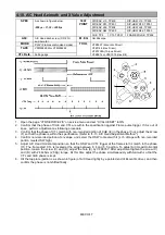
6. After finish the Linearity Adjustment, measure the numerical value of linearity and waving.
Waving Measurement Procedures
1. Press “SPACE” key to perform the Peak Hold in 30 seconds when linearity is displayed.
2. After finish the Peak Hold, press “SHIFT” and “ } ” key simultaneously on the Key Board, then the numerical
values of “Linearity” and “Waving” is displayed on left lower portion of screen. And confirm the numerical values
are in the specification. Also confirm the waving is same level from entrance side to exit side. If the “Linearity”
and “Waving” are out of specification and also it caused by insufficient limit of entrance or exit side of envelope,
adjust height of S1 and T1 post.
3. After this measurement is finished, press the ESC key to return to the main menu.
Information : How to save the LISTA Data
Linearity waveform data and measurement value of linearity and waving can be saved as one file data to PC.
1. Basically this operation should be performed after linearity and waving measurement is finished.
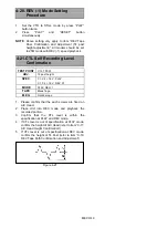
2. Select the item “<3> Data Save/Load” on the LISTA main menu, and select the item “<1> Save”.
3. The linearity waveform as Peak Hold is displayed on the screen, and message “File Name?” appears on the
screen. Then entry the File Name less than 8 letters. And after message “Comment?” appears on the screen,
then entry the Comment less than 20 letters. As comment, entry the Serial Number, Model Number, Head
Rotation Hours etc to use them for management of each VTR’s linearity data.
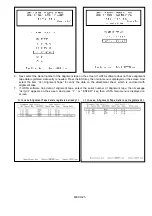
4. After completion of saving, select the item “<2> Load” of the item “<3> Data Save/Load”, then the saved File
Name appears on the screen. And select previously saved file to confirm the waveform and numerical value is
displayed correctly. By pressing “SHIFT” and “ } ” key simultaneously on the Key Board, the numerical values of
“Linearity” and “Waving” is displayed on left lower portion of screen.
POINT :
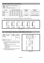
The part of left side of waveform (entrance side) is adjusted by height of S1 post and part of right side of
waveform (exit side) is adjusted by height of T1 post.
Lower part of above waveform of figure is displayed lead of Cylinder.
When the post driver is removed from upper part of post, linearity waveform may be changed.
After finish this adjustment, eject the tape and insert the tape again to confirm the shape of linearity waveform
isn’t changed.
Confirm this value
Summary of Contents for AJ-HDC27VP
Page 3: ... 3 ...
Page 4: ... 4 ...
Page 6: ... 6 ...
Page 7: ...Printed in Japan FCD0108NCKK71 ...
Page 136: ...ELE 25 9 TP VR and SW Location AUDIO LCD P C BOARD VEP84331B COMPONENT SIDE FOIL SIDE ...
Page 137: ...ELE 26 VIDEO OUT P C BOARD VEP23500B VTR SYSCON P C BOARD VEP86303C COMPONENT SIDE FOIL SIDE ...
Page 138: ...ELE 27 SERVO P C BOARD VEP82224B COMPONENT SIDE FOIL SIDE ...
Page 139: ...ELE 28 VIDEO MAIN P C BOARD VEP83462C COMPONENT SIDE FOIL SIDE ...
Page 140: ...ELE 29 FOIL SIDE DSP MAIN P C BOARD VEP23530B COMPONENT SIDE ...
Page 141: ...ELE 30 VTR MOTHER P C BOARD VEP80B10A RF EQ P C BOARD VEP87104B COMPONENT SIDE COMPONENT SIDE ...
Page 151: ...HEAD BUFFER BLOCK DIAGRAM BLK 6 ...
Page 152: ...BLK 7 RF EQ BLOCK DIAGRAM ...
Page 153: ...HD SDI TX VIDEO MAIN BLOCK DIAGRAM BLK 8 DSP MAIN DSP MAIN DSP MAIN DSP MAIN HD SDI TX ...
Page 155: ...SERVO BLOCK DIAGRAM BLK 10 ...
Page 157: ...VTR SYSCON SD CARD BLOCK DIAGRAM BLK 12 Q1 SD CARD CKK USED USED ...
Page 158: ...POWER MAIN SUB BLOCK DIAGRAM BLK 13 ...
Page 323: ...PRT 2 MECHANICAL CHASSIS ASSEMBLY 1 ...
Page 325: ...PRT 4 MECHANICAL CHASSIS ASSEMBLY 2 ...
Page 327: ...PRT 6 CHASSIS FRAME ASSEMBLY 1 ...
Page 329: ...PRT 8 CHASSIS FRAME ASSEMBLY 2 ...
Page 331: ...PRT 10 CHASSIS FRAME ASSEMBLY 3 ...
Page 333: ...PRT 12 CASSETTE COMPARTMENT ASSEMBLY ...
Page 335: ...PRT 14 PACKING PARTS ASSEMBLY ...
Page 387: ...HEAD BUFFER BLOCK DIAGRAM BLK 6 ...
Page 388: ...BLK 7 RF EQ BLOCK DIAGRAM ...
Page 389: ...HD SDI TX VIDEO MAIN BLOCK DIAGRAM BLK 8 DSP MAIN DSP MAIN DSP MAIN DSP MAIN HD SDI TX ...
Page 391: ...SERVO BLOCK DIAGRAM BLK 10 ...
Page 393: ...VTR SYSCON SD CARD BLOCK DIAGRAM BLK 12 Q1 SD CARD CKK USED USED ...
Page 394: ...POWER MAIN SUB BLOCK DIAGRAM BLK 13 ...
Page 399: ...CBA 5 FOIL SIDE CCD SENSOR P C BOARD VEP20854A FOIL SIDE IC101 E1 IC201 C1 IC301 A1 ...
Page 499: ...ELE 25 9 TP VR and SW Location AUDIO LCD P C BOARD VEP84331B COMPONENT SIDE FOIL SIDE ...
Page 500: ...ELE 26 VIDEO OUT P C BOARD VEP23500B VTR SYSCON P C BOARD VEP86303C COMPONENT SIDE FOIL SIDE ...
Page 501: ...ELE 27 SERVO P C BOARD VEP82224B COMPONENT SIDE FOIL SIDE ...
Page 502: ...ELE 28 VIDEO MAIN P C BOARD VEP83462C COMPONENT SIDE FOIL SIDE ...
Page 503: ...ELE 29 FOIL SIDE DSP MAIN P C BOARD VEP23530B COMPONENT SIDE ...
Page 504: ...ELE 30 VTR MOTHER P C BOARD VEP80B10A RF EQ P C BOARD VEP87104B COMPONENT SIDE COMPONENT SIDE ...
Page 554: ...PRT 2 MECHANICAL CHASSIS ASSEMBLY 1 ...
Page 556: ...PRT 4 MECHANICAL CHASSIS ASSEMBLY 2 ...
Page 558: ...PRT 6 CHASSIS FRAME ASSEMBLY 1 ...
Page 560: ...PRT 8 CHASSIS FRAME ASSEMBLY 2 ...
Page 562: ...PRT 10 CHASSIS FRAME ASSEMBLY 3 ...
Page 564: ...PRT 12 CASSETTE COMPARTMENT ASSEMBLY ...
Page 566: ...PRT 14 PACKING PARTS ASSEMBLY ...


