PhotoMOS
®
Cautions for Use
Panasonic Corporation 2022
Panasonic Corporation Electromechanical Control Business Division
industrial.panasonic.com/ac/e/
ASCTB65E 202201
Output Waveform (CC Type)
This product has the capacitor coupled isolation. Therefore, if output
waveform fluctuates along the time axis (e.g. AC waveform or
pulsating waveform), it may affect the operation of this product and
peripheral circuit. Please evaluate the device in the actual condition.
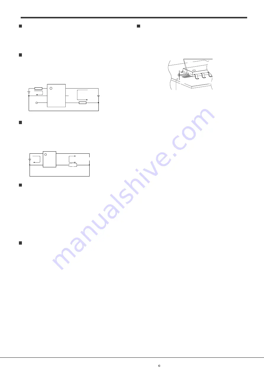
Continual DC bias (AQV259 and AQV258)
If a continual DC bias will be applied between the input and output,
the breakdown voltage of the switching element MOSFET on the
output side may degrade. Therefore, be sure to test the product
under actual conditions. Example of circuits that will cause
degradation of breakdown voltage of MOSFET is given below.
I
F
I
L
1
2
3
6
5
4
E
Load
Connections Between Input and Output (CC Type)
If you wish to use the product with a connection between input and
output, you may not obtain expected performance. Therefore,
please be sure to evaluate the device in the actual usage. A circuit
example is shown below that may negatively affect PhotoMOS
characteristics.
I
IN
I
L
V
L
(AC, DC)
V
IN
3
4
2
1
Load
Cleaning solvents compatibility
Cleaning the solder flux should use the immersion washing with an
organic solvent. If you have to use ultrasonic cleaning, please adopt
the following conditions and check that there are no problems in the
actual usage.
• Frequency: 27 to 29kHz
• Ultrasonic output: No greater than 0.25W/cm
2
*
• Cleaning time: 30s or less
• Others: Float PCB and the device in the cleaning solvent to
prevent from contacting the ultrasonic vibrator
* Applies to unit area ultrasonic output for ultrasonic baths
Notes for mounting
1) When different kinds of packages are mounted on PC boad,
temperature rise at soldering lead is highly dependent on
package size. Therefore, please set the lower temperature
soldering condition than the conditions of item “
■
Soldering”, and
confirm the temperature condition of actual usage before
soldering.
2) When soldering condition exceeds our recommendation, the
PhotoMOS
®
characteristics may be adversely affected. It may
occur package crack or bonding wire breaking because of
thermal expansion unconformity and resin strength reduction.
Please contact our sales office about the propriety of the
condition.
3) Please confirm the heat stress by using actual board because it
may be changed by board condition or manufacturing process
condition.
4) Solder creepage, wettability, or soldering strength will be affected
by the soldering condition or used soldering type. Please check
them under the actual production condition in detail.
5) Please apply coating when the device returns to a room
temperature.
Input wiring pattern
1) With AQY* or AQW* series avoid installing the input (LED side)
wiring pattern to the bottom side of the package if you require the
specified I/O isolation voltage (V
iso
) after mounting the PC board.
Since part of the frame on the output side is exposed, it may
cause fluctuations in the I/O isolation voltage.
(Output terminal side)
(Output terminal side)
(Input terminal side)
(Input terminal side)
Input wiring
pattern
Input wiring
pattern
May not allow the prescribed I/O withstand
voltage (Viso) to be achieved
Portion of output side frame
Portion of output side frame
* Excluding high I/O isolation voltage products and SSOP, SON, and TSON
packages
2) Exposed terminals are electrically connected to internal elements.
Be aware that contact with external circuits may cause
deterioration of insulation between input and output, leading to
destruction of internal elements.
3) If installed in proximity to other device, take care to avoid short
circuits between device, which may occur if exposed frames of
adjacent device come too close.
ー 10 ー