Stacking connector for high current
B01
–5–
ACCTB71E 201412-T
NOTES
1. Design of PC board patterns
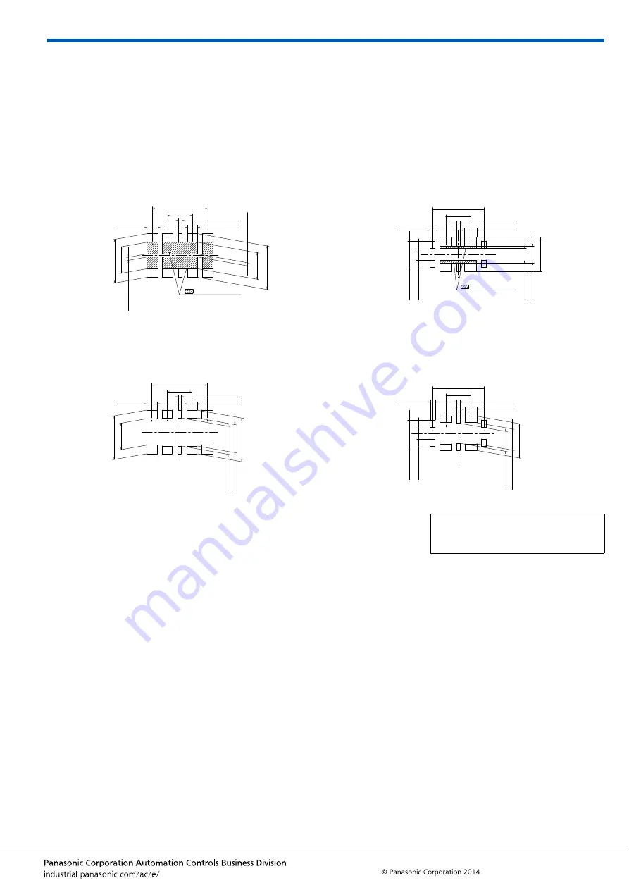
Conduct the recommended foot pattern design, in order to
preserve the mechanical strength of terminal solder areas.
2. Recommended PC board and metal mask patterns
In order to reduce solder and flux rise, solder bridges and other
issues make sure the proper levels of solder is used.
The figures to the right are recommended metal mask patterns.
Please use them as a reference.
• Socket (Mated height: 0.6 mm and 0.8 mm)
Recommended PC board pattern (TOP VIEW)
Recommended metal mask pattern
Metal mask thickness: When 100
μ
m
(Power contact opening ratio: 88%)
(Signal contact opening ratio: 83%)
(Metal-part opening ratio: 100%)
• Header (Mated height: 0.6 mm and 0.8 mm)
Recommended PC board pattern (TOP VIEW)
Recommended metal mask pattern
Metal mask thickness: When 100
μ
m
(Power contact opening ratio: 73%)
(Signal contact opening ratio: 75%)
(Metal-part opening ratio: 100%)
: Insulation area
2.80
±
0.03
1.70
±
0.03
0.20
±
0.03
0.22
±
0.03
0.66
±
0.03
3.56
±
0.03
1.60
±
0.03
0.70
±
0.03
2.80
±
0.03
1.70
±
0.03
0.20
±
0.03
2.80
±
0.03
1.80
±
0.03
1.80
±
0.03
0.20
±
0.03
0.64
±
0.03
3.56
±
0.03
1.60
±
0.03
0.70
±
0.03
2.80
±
0.03
1.70
±
0.03
Please refer to the latest product
specifications when designing your
product.
: Insulation area
3.30
±
0.03
1.60
±
0.03
0.22
±
0.03
0.78
±
0.03
0.32
±
0.03
2.20
±
0.03
1.08
±
0.03
0.80
±
0.03
1.71
±
0.03
0.74
±
0.03
3.30
±
0.03
1.60
±
0.03
0.20
±
0.03
0.76
±
0.03
2.20
±
0.03
1.36
±
0.03
1.28
±
0.03
1.71
±
0.03
0.74
±
0.03
0.32
±
0.03


