Page 1-17
GENERAL DESCRIPTION
1
1-4
Other Specification
1-4-1
Available Board Specification
Item
Specification
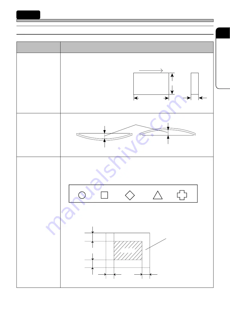
Board Size
Size
Max. : 460 (L)
×
360 (W)
Min. : 50 (L)
×
50 (W)
Thickness
0.5
≤
T
≤
3.0
Tolerance for
Board Warp
±
1.0 mm or less
Board Recognition
Mark
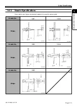
Examples of Mark Shape
Board recognition correction is performed on the basis of the positional relation be-
tween the recognition mark and the circuit pattern.
A certain contrast is required between the recognition mark and the board. (Binary
contrast image)
Mark Size and Background
A certain size of neutral area that is different from the mark is required for the back-
ground of mark.
a
≥
0.2 mm
433C-019E
444C-113E
Mark
Transport Direction
L (Length)
W (Width)
T (Thickness)
Warp
Cross Section of Board
Neutral Area
a
a
a
a
3F3C-IL012
1
2
3
4
5
( Unit : mm )
4H4C-E-OMA01-A01-00
Summary of Contents for CM301
Page 2: ......
Page 6: ...Page 4 4H4C E OMA00 B01 00 MEMO ...
Page 19: ...Page 17 SAFETY PRECAUTIONS Be sure to observe 4H4C E OMA00 A03 02 WARNING ...
Page 64: ...Page 1 20 MEMO 4H4C E OMA01 A01 01 ...
Page 78: ...Page 2 14 MEMO 4H4C E OMA02 A01 01 ...


