1
ABOUT LEAD FREE SOLDER (PbF)
2
2
FEATUERS
2
3
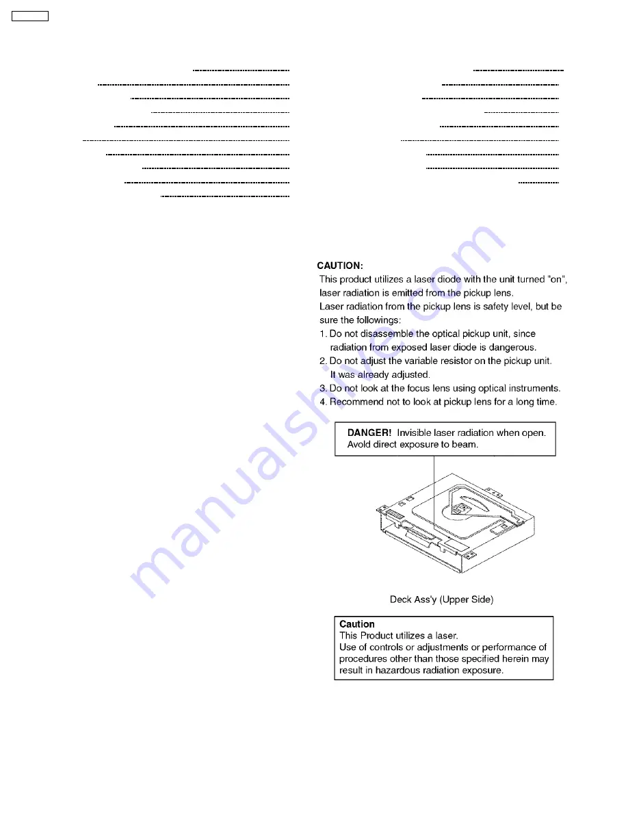
LASER PRODUCTS
2
4
REPLACEING THE FUSE
2
5
MAINTENANCE
3
6
NOTES
3
7
DIMENSIONS
3
8
WIRING CONNECTION
4
9
BLOCK DIAGRAM
5
10 TERMINALS DESCRIPTION
6
1 ABOUT LEAD FREE
SOLDER (PbF)
Distinction of PbF PCB:
PCBs (manufactured) using lead free solder will have a PbF
stamp on the PCB.
Caution :
•
•
•
•
Pb free solder has a higher melting point than standard
solder; Typically the melting point is 50 - 70°F (30 -
40°C)
higher.
Please
use
a
soldering
iron
with
temperature control and adjust it to 700 ± 20°F (370 ±
10°C). In case of using high temperature soldering iron,
please be careful not to heat too long.
•
•
•
•
Pb free solder will tend to splash when heated too high
(about 1100°F/600°C)
•
•
•
•
This lead free solder will be used for the products after
serial No. 1,000,001.
2 FEATUERS
•
•
•
•
18-FM, 6-AM presets with preset scan
•
•
•
•
Digital servo for reliable CD playback.
•
•
•
•
Removable face plate.
11 PACKAGE AND IC BLOCK DIAGRAM
8
12 REPLACEMENT PARTS LIST
12
13 EXPLODED VIEW (Unit)
16
14 CD PLAYER MECHANICAL PARTS LIST
17
15 EXPLODED VIEW (CD Deck)
18
16 WIRING DIAGRAM
19
17 SCHEMATIC DIAGRAM-1
23
18 SCHEMATIC DIAGRAM-2
25
19 SCHEMATIC DIAGRAM for printing with A4 size
27
3 LASER PRODUCTS
4 REPLACEING THE FUSE
Use fuses of the same specified rating (15A). Using different
substitutes or fuses with higher ratings, or connecting the
product directly without a fuse, could cause fire or damage to
the stereo unit.
CONTENTS
Page
Page
2
CQ-C1115N
Summary of Contents for CQ-C1115N
Page 4: ...8 WIRING CONNECTION 4 CQ C1115N ...
Page 5: ...9 BLOCK DIAGRAM 5 CQ C1115N ...
Page 9: ...IC1 C1BB00001089 9 CQ C1115N ...
Page 10: ...IC300 C1BB00000543 IC2 C1BB00001088 10 CQ C1115N ...
Page 11: ...IC701 C0DAZHF00004 11 CQ C1115N ...
Page 16: ...13 EXPLODED VIEW Unit 16 CQ C1115N ...
Page 18: ...15 EXPLODED VIEW CD Deck 18 CQ C1115N ...
Page 20: ...16 2 Main Block 2 E 4C316 BOTTOM VIEW CQ C1115N C1105W C1105H MAIN PCB 20 CQ C1115N ...
Page 21: ...16 3 Display Block E 4C317 TOP VIEW CQ C1115N DISPLAY PCB E 4C317 BOTTOM VIEW 21 CQ C1115N ...
Page 24: ...17 2 Main Block E 4C316B CQ C1115N C1105W C1105H MAIN BLOCK CQ C1115N 24 ...
Page 25: ...18 SCHEMATIC DIAGRAM 2 18 1 Display Block E 4C317 CQ C1115N DISPLAY BLOCK 25 CQ C1115N ...
Page 27: ...19 1 Main Block Left Side 19 SCHEMATIC DIAGRAM for printing with A4 size 27 CQ C1115N ...


