background image

27

10.2. Replacement Parts List

Notes :

1. Be sure to make your orders of replacement parts accord-

ing to this list.

2. Important safety notice: Components, identified by 

mark have special characteristics important for safety.
When replacing any of these components, use only man-
ufacturer's specified parts.

3. Location keys in the remarks column indicates the gen-

eral location of the parts shown in the exploded drawing,
as in a road map.

4. The marking (RTL) indicates that Retention Time is lim-

ited for this item. After the discontinuation of assembly in
production, the item will continue to be available for a
specific period of time. The retention period of availability
is dependent on the type of assembly, and in accordance
with the laws governing part and product retention. After
the end of this period, the assembly will no longer be
available.

• Order intake period is basically six months after the first

shipment.

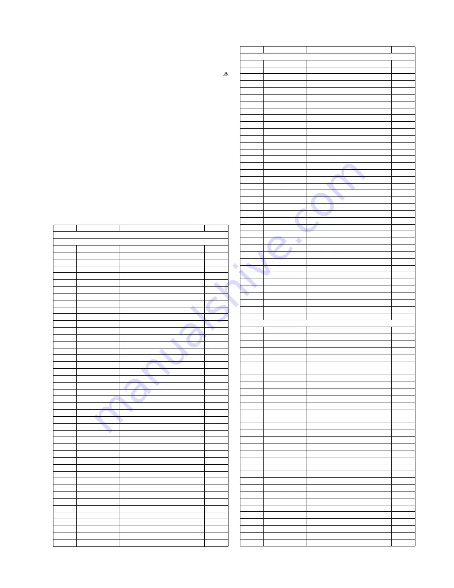
Ref. No.

Part No.

Part Name & Description

Remarks

[E3108] Main Block

IC's AND TRANSISTORs

IC201

C1BB00000796

IC

IC221

C1BB00001131

IC

IC231

C0JBZS000003

IC

IC271

C1ZAZ0001450

IC

IC401

C1BB00001045

IC

IC501

C1BB00000960

IC

IC601

C2CBKG000037

IC

IC630

C0JBAA000372

IC

IC650

C0JBAA000372

IC

IC670

YEAMC14584BE

IC

IC701

C0DAZHF00004

IC

IC702

C0EBZ0000035

IC

IC730

C0DAEKG00002

IC

IC752

C0CBCBG00012

IC

IC755

C0DBZGD00040

IC

IC760

C0GBG0000032

IC

IC790

C0CBCYG00004

IC

PA51

C5BA00000123

Electronic Tuner

Q55

B1GDGFEH0001

Transistor

Q56

B1AAEC000002

Transistor

Q66

B1ABCF000187

Transistor

Q220

B1GBCFNN0004

Transistor

Q235

B1GBHBEA0004

Transistor

Q241

B1GBHBEA0004

Transistor

Q320

B1GBCFNN0004

Transistor

Q335

B1GBHBEA0004

Transistor

Q341

B1GBHBEA0004

Transistor

Q346

B1GBHBEA0004

Transistor

Q371

B1GBCFNN0004

Transistor

Q372

YEANC114YKX

Transistor

Q376

B1GBCFNN0004

Transistor

Q411

B1CBGF000005

Transistor

Q630

B1GBCFNN0004

Transistor

Q633

B1GDCFJJ0002

Transistor

Q650

YEANC114YKX

Transistor

Q651

YEANC114YKX

Transistor

Q652

YEANC114YKX

Transistor

Q680

B1GDGFEH0001

Transistor

Q681

B1GDCFJJ0002

Transistor

Q701

B1BACF000026

Transistor

Q760

B1GBCFNN0004

Transistor

Q791

B1GBNCEJ0003

Transistor

Q793

YEANC114YKX

Transistor

DIODEs

D201

B0JCME000012

Diode

D202

B0JCME000012

Diode

D203

B0JCME000012

Diode

D204

B0JCME000012

Diode

D301

B0JCME000012

Diode

D302

B0JCME000012

Diode

D303

B0JCME000012

Diode

D304

B0JCME000012

Diode

D346

B0JCMC000004

Diode

D504

B0BC5R000020

Diode

D601

B0JCMC000004

Diode

D630

B3AAB0000143

Diode

D631

B0BC5R600003

Diode

D632

MA152WATX

Diode

D635

B0BC5R600003

Diode

D636

B0BC5R600003

Diode

D637

B0BC5R600003

Diode

D638

B0BC5R600003

Diode

D639

B0BC5R600003

Diode

D670

B0JCMC000004

Diode

D680

MA3X152A0L

Diode

D701

YEADDAM3MA47 Diode

D702

MA736TX

Diode

D703

B0BC5R7A0062

Diode

D704

B0JCMC000004

Diode

D705

YEADSR1544TL

Diode

D706

YEADSR1544TL

Diode

D707

YEADRB051L40

Diode

D708

MA736TX

Diode

D710

B0JCMC000004

Diode

D715

MA3X152A0L

Diode

D716

MA721TX

Diode

D751

YEADSR1544TL

Diode

D752

YEADSR1544TL

Diode

D760

B0BC5R000020

Diode

D761

B0BC3R0A0058

Diode

CAPACITORs

C50

YECUS1H100CC

Ceramic, 10PF 50WV

C52

YECUS1H470JC

Ceramic, 47PF 50WV

C53

F1J1H103A513

Ceramic, 0.01

µ

F 50WV

C54

F2A1A221A449

Electrolytic, 220

µ

F 10WV

C55

F1J1H103A513

Ceramic, 0.01

µ

F 50WV

C56

F3F1E105A018

Tantalum, 1

µ

F 25WV

C57

F2A1A101A450

Electrolytic, 100

µ

F 10WV

C61

YECUS1H183KX

Ceramic, 0.018

µ

F 50WV

C62

YECUS1H183KX

Ceramic, 0.018

µ

F 50WV

C65

F1J1H1020024

Ceramic, 1000PF 50WV

C66

F1J1H471A672

Ceramic, 470PF 50WV

C206

F2A1C100A502

Electrolytic, 10

µ

F 16WV

C213

F1J1A2250004

Ceramic, 2.2

µ

F 10WV

C215

F1J1A2250004

Ceramic, 2.2

µ

F 10WV

C217

YECUS1C334KX

Ceramic, 0.33

µ

F 16WV

C220

F1J1C225A138

Ceramic, 2.2

µ

F 16WV

C237

F1J1C225A138

Ceramic, 2.2

µ

F 16WV

C242

F1J1C225A138

Ceramic, 2.2

µ

F 16WV

C271

F1J1H472A675

Ceramic, 4700PF 50WV

C272

F1J1H472A675

Ceramic, 4700PF 50WV

C274

F2A1C470A630

Electrolytic, 47

µ

F 16WV

C275

F1J1C1050013

Ceramic, 1

µ

F 16WV

C278

YECUS1E104ZF

Ceramic, 0.1

µ

F 25WV

C279

F2A1C4720027

Electrolytic, 4700

µ

F 16WV

C281

F1K1C1060001

Ceramic, 10

µ

F 16WV

C282

YECUZ1C104KX

Ceramic, 0.1

µ

F 16WV

C283

F1K1C1060001

Ceramic, 10

µ

F 16WV

C296

F1K1C4740009

Ceramic, 0.47

µ

F 16WV

C297

F1K1C4740009

Ceramic, 0.47

µ

F 16WV

C306

F2A1C100A502

Electrolytic, 10

µ

F 16WV

C313

F1J1A2250004

Ceramic, 2.2

µ

F 10WV

C315

F1J1A2250004

Ceramic, 2.2

µ

F 10WV

Ref. No.

Part No.

Part Name & Description

Remarks

Summary of Contents for CQ-C7353N

Page 1: ...3N WMA MP3 CD Player Receiver TABLE OF CONTENTS PAGE PAGE 1 Service Navigation 2 2 Specifications 3 3 Features 4 4 Technical Descriptions 5 5 Disassembly and Assembly Instructions 10 6 Block Diagram 13 7 Wiring Connection Diagram 16 8 Schematic Diagram 17 9 Printed Circuit Board 21 10 Exploded View and Replacement Parts List 26 11 Schematic Diagram for Printing with A4 Size 37 ...

Page 2: ...solder will be used for the products after serial No 1 000 001 1 2 Laser Products 1 3 Replacing the Fuse Use fuses of the same specified rating 15 amps Using different substitutes or fuses with higher ratings or connecting the unit directly without a fuse could cause fire or damage to the stereo unit 1 4 Maintenance Your product is designed and manufactured to ensure a mini mum of maintenance Use ...

Page 3: ... W H D 178 50 155mm Weight 1 6 kg CD Player Sampling Frequency 8 times Oversampling DA Converter 4 DAC System Pick Up Type Astigma 3 beam Light Source Semiconductor Laser Wave Length 790 nm Frequency Response 20 Hz 20 kHz 1 dB Signal to Noise Ratio 96 dB Total Harmonic Distortion 0 01 1 kHz Wow and Flutter Below Measurable Limits Channel Separation 85 dB FM Stereo Radio Frequency Range 87 5 MHz 10...

Page 4: ...tional adapter allows you to connect the optional Panasonic DVD changer unit CX DH801N The optional adapter allows you to connect the optional Panasonic CD changer unit CX DP880 The optional adapter allows you to connect the optional iPod series SQ7 7 Band Sound Quality Customize the Display Customize Function MP3 WMA Playback from CD R RW ...

Page 5: ...ncoming detec tion I 5 2 5 2 5 2 44 HUB CNT Request of hub connection check O 0 0 0 45 CD SW1 Disc detection switch 1 I 0 0 0 46 CD SW2 Disc detection switch 2 I 0 0 0 47 MOD0 Operating mode control 0 from Flash writer I 5 1 5 1 5 1 48 MOD1 Operating mode control 1 pulled up to H 5 1 5 1 5 1 49 MOD2 Operating mode control 2 from Flash writer I 0 0 0 50 H STANDBY Standby control from exter nal I 5 ...

Page 6: ...ontrol 2 from Flash writer I 0 50 NC Not connected 51 ROTARY 1 Volume up detection from Rotary encoder I 2 5 Pin No Port Description I O V FM AM CD 52 ROTARY 2 Volume down detection from Rotary encoder I 2 5 53 NC Not connected 54 NC Not connected 55 NC Not connected 56 NC Not connected 57 NC Not connected 58 FLASH CE Chip enable for Flash memory O 3 4 59 LCD CS LCD chip select O 3 4 60 LED R 61 N...

Page 7: ...CCE DSP IC CCE O 2 6 31 BUCK DSP IC CK O 2 8 32 BUS3 DSP IC BUS3 O 2 8 33 BUS2 DSP IC BUS2 O 2 8 34 BUS1 DSP IC BUS1 O 2 8 35 BUS0 DSP IC BUS0 O 2 9 36 RESET SW Mechanics deck REST SW input I 3 2 37 SW1 Mechanics deck SW1 input I 0 38 SW2 Mechanics deck SW2 input I 0 39 CONT P13 DSP IC power control 1 O 3 2 40 Not Connected 41 Not Connected 42 Not Connected 43 CONT P17 DSP IC power control 2 O 3 2...

Page 8: ...8 4 2 IC Block Diagram 4 2 1 Main Block IC201 C1BB00000796 IC231 C0JBZS000003 IC670 YEAMC14584BE IC730 C0DAEKG00002 IC701 C0DAZHF00004 IC755 C0DBZGD00040 ...

Page 9: ...9 IC760 C0GBG0000032 4 3 Display Block IC902 C0EBF0000374 4 4 CD Servo Block IC401 IC403 YESAM341 IC402 YESAM342 ...

Page 10: ...release button 3 Remove the screw and take off the Upper cover 4 Remove the 3 screws and take off the CD deck 5 Remove the flexible PCB AP2 from the CN601 E 3108a 6 Remove the screw from the Drive Mechanism Ass y and remove the flexible PCB case 7 Remove the flexible PCB AP2 from the CN1 Trim plate Release button Upper cover CD deck Drive Mechanism Ass y Flexible PCB case CN1 AP2 Removable face pl...

Page 11: ...11 5 2 How to Install the Main P C B of the Electric Display ...

Page 12: ...12 ...

Page 13: ... 32 24 17 CD L CD R CD8V CD3 3V CD IN CD FS CD SCK CD SI CD SO CD RST MUTE CN651 R CH IC752 Q650 IC650 CD8V BATT 5V REG LEVEL SHIFT 16 17 9 10 13 14 4 3 6 5 7 8 1 2 To CD DECK CD SW1 CD SW2 Q652 Q651 Q320 IC231 Q371 Q701 REG 11 6 7 8 3 4 2 5 10 12 14 BATT VDD5V ACC IC701 POWER SUPPLY ANT B CD8V AUDIO9V SW5V ILM10V ACC DECK V CONT ANT CONT 1 MAIN CONT IC271 POWER AMP 25 22 4 5 3 6 20 23 21 14 12 CL...

Page 14: ...P905 Q941 943 LED B LED G LED R 6 5 60 D907 IC902 RESET 12 10 8 1 13 13 11 9 2 2 5 6 4 1 9 8 10 7 5 4 6 3 12 11 3 IC670 CN680 4 1 3 2 8 6 7 MOTOR DRIVE 17 16 OUT1 OUT2 IC760 9 5 21 18 20 VR Q760 VOLT CONT CN760 1 2 BATT ILM10V V CONT1 SYS ID1 SYS ID2 MAIN CONT2 CH REM HUB CNT EVENT CH STB CH CLK CH DATA SO MOD2 MOD0 RST SI CLK AMP CONT FP MOTOR1 FP MOTOR2 54 77 78 22 20 27 28 44 43 19 58 57 4 75 5...

Page 15: ...IVE MUTE MUTE RST 43 37 38 36 39 5 29 2 3 SW1 SW2 RESET TVD ESC FOD TE FE RF TRD SERVO CTL IC201 RF AMP SERVO DSP 92 91 99 98 97 95 EFM DEM REG CD8V DSP3 3V REG CD3 3V 1 5V REG ADC 15 18 14 9 24 23 18 36 I 39 32 I 35 34 40 41 43 BUCK ZDET BUS 0 3 CCE STBY 14 53 SBSY X201 VCOM LD EJ RST LD MT CNT XI XO CN101 CN102 Lch Rch CD3 3V DC8V 10 DC8V 8 12 CD SI 7 11 CD SO To MAIN CN651 1 SW1 2 SW2 6 13 CD S...

Page 16: ...CN302 CN202 CN255 CN351 L R L R L R L R PRE OUT REAR S W OUT AUX1 IN PRE OUT FRONT CN701 CP670 CN255 CN351 CN302 CN202 1 4 1 4 1 4 1 4 ANT51 CN651 CN670 17 18 1 18 1 1 7 2 17 2 Loading Feed Moter Reset SW Optical Pic Up Ass y CN101 SW1 SW2 CN102 Spindle Motor 16 1 CD Servo P C B 3032 14 35 Main P C B E 3108a CN1 16P CN601 16P CN760 2P Drive Mechanism Ass y AP2 1 16 2P CN680 Display P C B E 9782a L...

Page 17: ...17 8 Schematic Diagram 8 1 Main 1 Block ...

Page 18: ...18 8 2 Main 2 Block ...

Page 19: ...19 8 3 Display Block ...

Page 20: ...2 2 2 3 1 6 1 6 1 6 1 6 1 6 1 5 1 5 1 7 0 0 0 1 5 1 6 0 0 0 1 6 2 5 1 8 3 1 0 7 9 3 5 4 1 4 0 3 4 0 0 7 9 1 7 1 1 1 4 1 6 3 2 3 2 3 2 8 0 3 3 0 1 6 1 6 0 0 0 0 0 0 0 0 0 7 1 5 0 0 0 0 0 0 0 0 0 1 5 0 0 1 6 1 6 1 6 1 6 1 6 3 3 3 3 3 3 2 9 2 9 2 8 2 8 2 8 1 6 3 3 3 3 1 5 3 2 2 6 1 4 1 6 0 6 1 6 1 6 1 6 1 6 1 6 1 6 1 6 1 8 1 8 1 3 1 3 3 3 3 3 2 5 0 2 1 8 1 8 1 5 1 5 0 0 2 0 2 0 2V DIV 5ms DIV 2V DIV ...

Page 21: ...21 9 Printed Circuit Board 9 1 Main Block Top View ...

Page 22: ...22 9 2 Main Block Bottom View ...

Page 23: ...23 9 3 Display Block ...

Page 24: ...24 9 4 CD Interface Block Top View ...

Page 25: ...25 9 5 CD Interface Block Bottom View ...

Page 26: ... 53 80 81 81 35 35 36 81 40 81 81 50 76 80 76 51 45 44 44 41 42 43 CN302 CN202 35 35 CN255 CN351 80 4 CD Deck Ass y 38 LED P C B E 9782b 5 CP905 CN902 CP904 71 To Main P C B E 3108a CN701 Installation Parts Power Connector A A SW901 CN901 CN601 CN760 HP2 CN701 CN680 CN255 CN351 CN302 CN202 CN651 CN670 SW601 SW602 HP1 LCD901 75 75 3 26 25 21 23 22 24 16 29 27 28 52 52 55 78 77 54 1 Display P C B E ...

Page 27: ...00026 Transistor Q760 B1GBCFNN0004 Transistor Q791 B1GBNCEJ0003 Transistor Q793 YEANC114YKX Transistor DIODEs D201 B0JCME000012 Diode D202 B0JCME000012 Diode D203 B0JCME000012 Diode D204 B0JCME000012 Diode D301 B0JCME000012 Diode D302 B0JCME000012 Diode D303 B0JCME000012 Diode D304 B0JCME000012 Diode D346 B0JCMC000004 Diode D504 B0BC5R000020 Diode D601 B0JCMC000004 Diode D630 B3AAB0000143 Diode D6...

Page 28: ...CUS1C104KX Ceramic 0 1µF 16WV C609 F1J1A106A023 Ceramic 10µF 10WV C610 YECUS1C104KX Ceramic 0 1µF 16WV C612 F1H1H120A231 Ceramic 12PF 50WV C613 F1H1H120A231 Ceramic 12PF 50WV C631 F2A1H4R7A632 Electrolytic 4 7µF 50WV Ref No Part No Part Name Description Remarks C632 YECUS1E104ZF Ceramic 0 1µF 25WV C633 F2A1C470A630 Electrolytic 47µF 16WV C634 F1H1E103A011 Ceramic 0 01µF 25WV C635 F1J1H103A513 Cera...

Page 29: ...rt Name Description Remarks R302 ERJ3GEYJ152V Chip 1 5kΩ 1 16W R303 ERJ3GEYJ103V Chip 10kΩ 1 16W R313 ERJ6GEYJ562 Chip 5 6kΩ 1 10W R314 ERJ6GEYJ103 Chip 10kΩ 1 10W R315 ERJ3GEYJ472V Chip 4 7kΩ 1 16W R316 ERJ3GEYJ123V Chip 12kΩ 1 16W R317 ERJ3GEYJ183V Chip 18kΩ 1 16W R320 ERJ3GEYJ750V Chip 75Ω 1 16W R321 ERJ3GEYJ153V Chip 15kΩ 1 16W R323 ERJ3GEYJ102V Chip 1kΩ 1 16W R324 ERJ3GEYJ103V Chip 10kΩ 1 16W...

Page 30: ... 1 16W R690 ERJ3GEYJ561V Chip 560Ω 1 16W R701 ERJ6GEYJ102 Chip 1kΩ 1 10W R702 ERJ3GEYJ224V Chip 220kΩ 1 16W R703 ERJ6GEYJ473 Chip 47kΩ 1 10W R704 ERJ8GEYJ4R7V Chip 4 7Ω 1 8W R705 ERJ6GEYJ682 Chip 6 8kΩ 1 10W R715 ERJ3GEYJ472V Chip 4 7kΩ 1 16W R716 ERJ6GEYJ473 Chip 47kΩ 1 10W R717 ERJ3GEYJ433V Chip 43kΩ 1 16W R719 ERJ3GEYJ684V Chip 680kΩ 1 16W R722 ERJ3GEYJ104V Chip 100kΩ 1 16W R732 ERJ6ENF1802V Ch...

Page 31: ...918 ERJ3GEYJ184V Chip 180kΩ 1 16W R923 ERJ3GEYJ473V Chip 47kΩ 1 16W R924 ERJ3GEYJ104V Chip 100kΩ 1 16W R925 ERJ3GEYJ302V Chip 3kΩ 1 16W R928 ERJ3GEYJ222V Chip 2 2kΩ 1 16W R929 ERJ3GEYJ122V Chip 1 2kΩ 1 16W Ref No Part No Part Name Description Remarks R932 ERJ3GEYJ101V Chip 100Ω 1 16W R933 ERJ6GEYJ751V Chip 750Ω 1 10W R934 ERJ3GEYJ103V Chip 10kΩ 1 16W R935 ERJ3GEYJ103V Chip 10kΩ 1 16W R936 ERJ3GEYJ...

Page 32: ...FE1310577 Button TUNE TRACK Cap 21 YEFK061410 Shading Cover 22 YEFV023497 Optical Shade 23 YEFX0013229 Transparent Plate 24 YEFV023498 Optical Shade 25 YEFE1310573 Button SRC 26 YEFE1310574 Button MENU BAND D 27 YEFE1310575 Button EJ TA SQ MUTE 28 YEFE1310579 Button RELEASE 29 YEFX0053029 Spring RELEASE 35 YEFR041000 Cap 36 YEFM031551 Laser Seal 38 YEFM031656 Laser Seal 40 YEFA07669 Front Plate St...

Page 33: ...33 10 3 Exploded View CD Deck GFX9995891 G F CD Servo P C B 3032 14 35 ...

Page 34: ...68pF 50WV C226 YESCC439 Ceramic 0 1µF 25WV C227 YESCC439 Ceramic 0 1µF 25WV C228 YESCC439 Ceramic 0 1µF 25WV C229 YESCC439 Ceramic 0 1µF 25WV C230 YESCC442 Ceramic 0 01µF 50WV C231 YESCC442 Ceramic 0 01µF 50WV C232 YESCC388 Electrolytic 100uF 16WV C233 YESCC388 Electrolytic 100uF 16WV C234 YESCC439 Ceramic 0 1µF 25WV C235 YESCC442 Ceramic 0 01µF 50WV C236 YESCC439 Ceramic 0 1µF 25WV C237 YESCC432 ...

Page 35: ...e 2 YESFX046137 Top Cover 3 YERFS04003 Damper F 4 YERFS04004 Damper R 11 YESFA01075 Chassis Rivet Ass y 12 YERFX046001 Change Plate Rivet Ass y 13 YERFX007001 Clamper Ass y 14 YESAK01047 Spindle Motor Ass y 15 YERFX046002 Clamper Arm 16 YERFX005001 Change Gear Spring 17 YERFX03001 Change Gear 2 18 YERFX03002 Feed Gear 19 YERFX03003 Feed Rack 20 YERFX046003 Changer Lock Lever 21 YERFW04001 Feed Swi...

Page 36: ...w 2 4 121 YERJW01001 P Washer 3 5 8 0 3 122 YERJW01002 HL Washer 1 85 5 0 13 123 YERJW01003 Lumilar Washer 3 1 6 0 1 124 YEJE01028 E Ring S 1 5 125 YERJW01005 P Washer 2 1 4 0 13 Ref No Part No Part Name Description Remarks ...

Page 37: ...37 11 Schematic Diagram for Printing with A4 Size 11 1 Main 1 Block Left Side ...

Page 38: ...38 11 2 Main 1 Block Right Side ...

Page 39: ...39 11 3 Main 2 Block Left Side ...

Page 40: ...40 11 4 Main 2 Block Right Side ...

Page 41: ...41 11 5 Display Block Left Side ...

Page 42: ...42 11 6 Display Block Right Side ...

Page 43: ...0 0 1 6 2 5 1 8 3 1 0 7 9 3 5 4 1 4 0 3 4 0 0 7 9 1 7 1 1 1 4 1 6 3 2 3 2 3 2 8 0 3 3 0 1 6 1 6 0 0 0 0 0 0 0 0 0 7 1 5 0 0 0 0 0 0 0 0 0 1 5 0 0 1 6 1 6 1 6 1 6 1 6 3 3 3 3 3 3 2 9 2 9 2 8 2 8 2 8 1 6 3 3 3 3 1 5 3 2 2 6 1 4 1 6 0 6 1 6 1 6 1 6 1 6 1 6 1 6 1 6 1 8 1 8 1 3 1 3 3 3 3 3 2 5 0 2 1 8 1 8 1 5 1 5 0 0 2 0 2 0 8V 3 3V 8V 3 3V CD L R The following symbols are shown on the schematic diagra...

Page 44: ...SAM342 YESAM337 0 0 3 2 3 2 3 2 3 2 3 2 3 2 2 6 2 8 3 0 1 3 1 3 0 0 2 9 0 0 0 0 3 2 3 2 3 2 3 2 0 0 2 1 0 3 2 3 0 3 2 3 2 3 2 2 9 2 8 2 8 0 0 0 0 0 5 2 8 3 3 3 2 8 0 0 3 2 3 2 0 1 5 3 2 0 1 5 3 2 2V DIV 5ms DIV 2V DIV 5ms DIV 2V DIV 1ms DIV 0 5V DIV 0 1µs DIV 8V L R L R R L 3 3V 3 3V 3 3V 3 3V 3 3V 3 3V 3 3V 3 3V 3 3V 8V 8V 8V ...

Page 45: ...45 Printed in Japan 2007 2 K Recycled Paper ...

Reviews: