background image

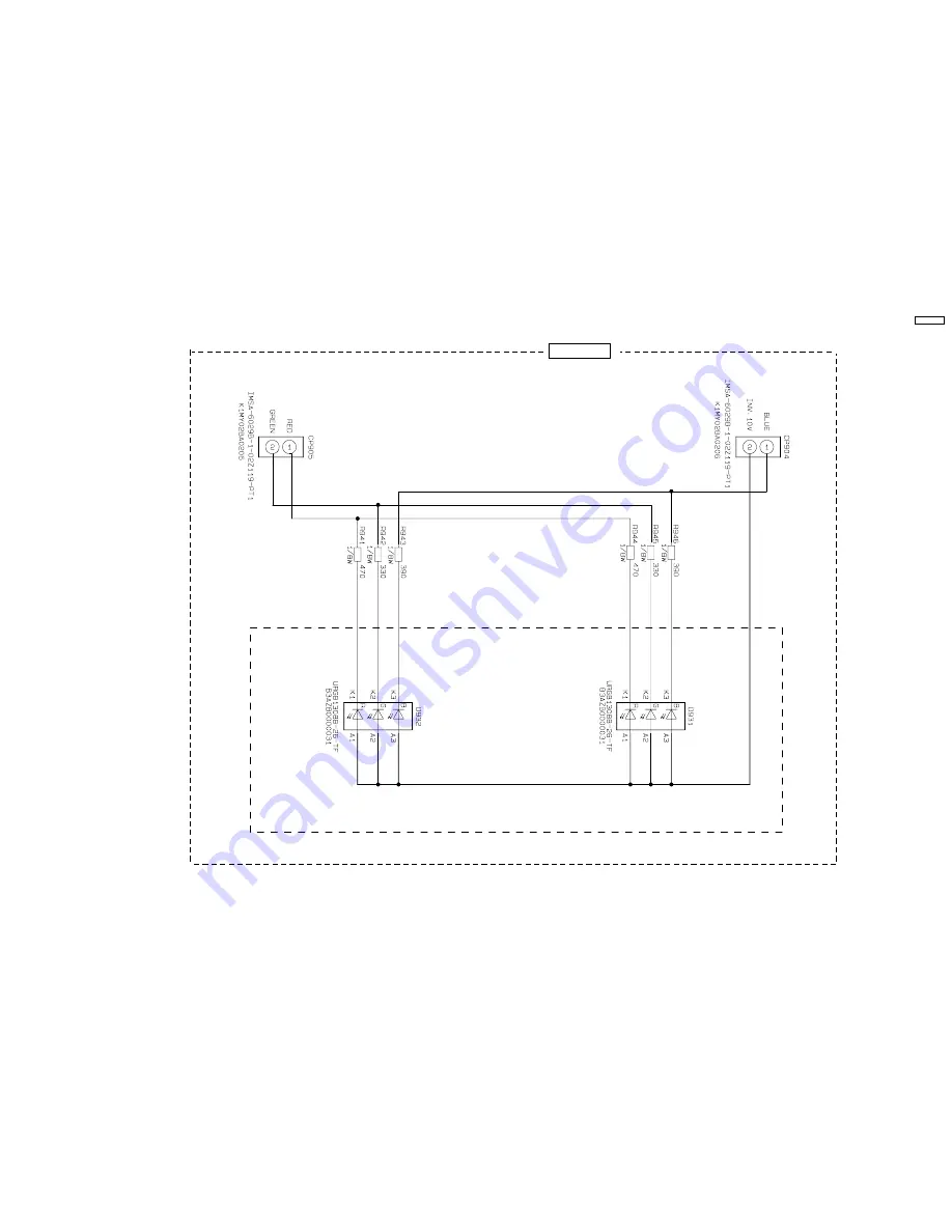
18.5. Display-b Block

E-4C311b

CQ-C7305N/C7405W DISPLAY BLOCK

CQ-C7405W

39

Summary of Contents for CQ-C7405W

Page 1: ...io Frequency Range 531kHz 1 602kHz Usable Sensitivity 28dB µV S N 20dB CD Player Sampling Frequency 8 Times Oversampling DA Converter 4 DAC System 2006 Matsushita Electric Industrial Co Ltd All rights reserved Unauthorized copying and distribution is a violation of law CQ C7405W WMA MP3 AAC CD Player Receiver Pick up Type Astigma 3 Beam Light Source Semiconductor Laser Wave Length 790 nm Frequency...

Page 2: ...CTION 4 9 BLOCK DIAGRAM 5 10 DISASSEMBLY INSTRUCTIONS 9 11 TERMINALS DESCRIPTION 12 12 IC BLOCK DIAGRAM 16 13 REPLACEMENT PARTS LIST 19 14 EXPLODED VIEW Unit 25 15 CD PLAYER PARTS LIST 26 16 EXPLODED VIEW CD PLAYER 28 17 WIRING DIAGRAM 29 18 SCHEMATIC DIAGRAM 35 19 SCHEMATIC DIAGRAM for printing with A4 size 41 CONTENTS Page Page 2 CQ C7405W ...

Page 3: ...c DVD changer unit CX DH801U The optional adapter allows you to connect the optional Panasonic CD changer unit CX DP880 The optional adapter allows you to connect the optional iPod series SQ7 7 Band Sound Quality Customize the Display Customize Function MP3 WMA AAC Playback from CD R RW 3 REPLACEING THE FUSE Use fuses of the same specified rating 15 amps Using different substitutes or fuses with h...

Page 4: ...8 WIRING CONNECTION 4 CQ C7405W ...

Page 5: ...9 BLOCK DIAGRAM 9 1 Main 1 Block CQ C7405W 5 ...

Page 6: ...9 2 Main 2 Block CQ C7405W 6 ...

Page 7: ...9 3 Display Block CQ C7405W 7 ...

Page 8: ...9 4 CD Servo Block CQ C7405W 8 ...

Page 9: ...10 DISASSEMBLY INSTRUCTIONS 10 1 How to Remove the Flexible PCB AP2 9 CQ C7405W ...

Page 10: ...10 2 How to Install the Main P C B of the Electric Display 10 CQ C7405W ...

Page 11: ...11 CQ C7405W ...

Page 12: ...ng mode control 0 from Flash writer I 5 2 5 2 5 2 48 MOD1 Operating mode control 1 pulled up to H I 5 2 5 2 5 2 49 MOD2 Operating mode control 2 from Flash writer I 0 0 0 50 H_STANDBY Standby control from external I 5 2 5 2 5 2 Pin No Port Description I O FM AM CD 51 DCDC_CONT Not connected O 0 0 0 52 FP_MOTOR1 Open Close of Front panel 1 O 5 1 5 1 5 1 53 FP_MOTOR2 Open Close of Front panel 2 O 5 ...

Page 13: ...1 IRQ1 NC I 3 8 47 MD0 MODE SET 0 I 3 5 48 MD1 MODE SET 1 I 3 5 49 MD2 MODE SET 2 I 0 50 P82 IRQ2 NC O 51 P83 IRQ3 Volume up detection from Rotary encoder I 3 2 Pin No Port Description I O V 52 P84 IRQ4 Volume down detection from Rotary encoder I 3 2 53 P85 IRQ5 NC O 54 P86 IRQ6 NC O 55 P87 IRQ7 NC O 56 P90 SIN1 CS0 NC O 57 P91 SOT1 CS1 NC O 58 P92 SCK1 CS 2 chip enable for Flash memory O 3 5 59 P...

Page 14: ... 65 68 P42 N C 0 0 69 FOP FOP 1 65 Pin No Port Description Play V Stop V 70 P43 N C 0 0 71 AVSS2 AVSS2 0 0 72 OSCIN OSCIN 1 65 1 65 73 CTRCRS CTRCRS 1 6 1 6 74 VREF VREF 1 65 1 65 75 E E 2 1 1 65 76 F F 2 1 1 65 77 D D 1 8 1 65 78 B B 1 8 1 65 79 C C 1 8 1 65 80 A A 1 8 1 65 81 PD PD 0 17 0 82 LD LD 2 5 3 3 83 CENV CENV 1 9 1 5 84 RFENV RFENV 1 7 1 7 85 RFOUT RFOUT 1 1 1 6 86 RFIN RFIN 1 8 1 8 87 ...

Page 15: ...O2 DRIVER CH2 OUTPUT O 4 6 4 6 4 6 4 6 13 VO1 DRIVER CH1 OUTPUT O 4 4 4 6 4 6 4 6 14 VO1 DRIVER CH1 OUTPUT O 4 8 4 6 4 6 4 6 15 VO4 DRIVER CH4 OUTPUT O 3 9 3 9 0 2 7 4 16 VO4 DRIVER CH4 OUTPUT O 3 9 3 9 7 4 0 2 17 VO3 DRIVER CH3 OUTPUT O 4 2 3 9 3 9 3 9 18 VO3 DRIVER CH3 OUTPUT O 3 6 3 9 3 9 3 9 19 GND GND 0 0 0 0 20 MUTE4 CH4 MUTE OUTPUT O 0 0 3 3 3 3 21 PowVcc2 Vcc CH3 CH4 8 8 8 22 PreVcc PreVcc...

Page 16: ...IC201 C1BB00000796 IC670 C0JBAZ000904 IC252 C0ABCA000121 IC271 C1ZAZ0001486 12 IC BLOCK DIAGRAM 12 1 Main Block 16 CQ C7405W ...

Page 17: ...IC251 C0ABBA000221 IC701 C0DAZHF00004 IC755 C0DBZGD00040 IC401 C1BB00001045 17 CQ C7405W ...

Page 18: ...IC760 C0GBG0000032 IC752 C0CBCBG00012 IC770 C0DBAHG00020 18 CQ C7405W ...

Page 19: ... No Part No Part Name Description Remarks Q633 B1GDCFJJ0002 Transistor T Q650 B1GBCFJN0004 Transistor T Q651 B1GBCFJN0004 Transistor T Q652 B1GBCFJN0004 Transistor T Q680 B1GDGFEH0001 Transistor T Q681 B1GDCFJJ0002 Transistor T Q701 B1BACF000026 Transistor T Q760 B1GBCFNN0004 Transistor T Q771 B1ABCF000187 Transistor T Q791 B1GBNCEJ0003 Transistor T Q793 B1GBCFJN0004 Transistor T T DIODEs D201 B0E...

Page 20: ... T C387 F1K1C106A098 Ceramic 10MFD 16WV T C388 F1K1C106A098 Ceramic 10MFD 16WV T Ref No Part No Part Name Description Remarks C389 F1K1C106A098 Ceramic 10MFD 16WV T C396 F1K1C474A098 Ceramic 0 47MFD 16WV T C397 F1K1C474A098 Ceramic 0 47MFD 16WV T C400 F1J1H102A733 Ceramic 1000pF 50WV T C401 F1J1H270A732 Chip 27pF 50WV T C402 F1J1H270A732 Chip 27pF 50WV T C403 F2A0J101A020 Electrolytic 100pF 6 3WV ...

Page 21: ...52 Chip 5 6 ohms 1 10W T R54 D0GD101JA017 Chip 100 ohms 1 10W T R55 D0GD331JA017 Chip 330 ohms 1 10W T R56 D0GD562JA017 Chip 5 6k ohms 1 10w T R59 D0GB104JA008 Chip 100k ohms 1 16W T R65 D0GD393JA017 Chip 39k ohms 1 10W T R202 D0GD152JA017 Chip 1 5k ohms 1 10W T R203 D0GD103JA017 Chip 10k ohms 1 10W T R213 D0GD562JA017 Chip 5 6k ohms 1 10w T R214 D0GD103JA017 Chip 10k ohms 1 10W T R215 D0GB472JA00...

Page 22: ... 16W T R628 D0GB103JA008 Chip 10k ohms 1 16W T R629 D0GF104JA014 Chip 100k ohms 1 8W T R631 D0GD821JA017 Chip 820 ohms 1 10W T R632 D0GD473JA017 Chip 47k ohms 1 10W T Ref No Part No Part Name Description Remarks R634 D0GD471JA017 Chip 470 ohms 1 10W T R638 D0GB102JA008 Chip 1k ohms 1 16W T R639 D0GB471JA008 Chip 470 ohms 1 16W T R640 D0GD561JA017 Chip 560 ohms 1 10w T R641 D0GB102JA008 Chip 1k ohm...

Page 23: ...ramic 10MFD 10WV T C928 F1H1H103A842 Ceramic 0 01MFD 50WV T C929 F1H1C104A107 Ceramic 0 1MFD 16WV T C931 F1J1A225A063 Ceramic 2 2MFD 10WV T C932 F1J1A225A063 Ceramic 2 2MFD 10WV T C933 F1J1A225A063 Ceramic 2 2MFD 10WV T C934 F1J1A225A063 Ceramic 2 2MFD 10WV T C935 F1J1A225A063 Ceramic 2 2MFD 10WV T C936 F1J1A225A063 Ceramic 2 2MFD 10WV T C937 F1K1C225A070 Ceramic 2 2MFD 16WV T C938 F1H1C104A107 Ce...

Page 24: ...No Part No Part Name Description Remarks CN1 K1NZ16H00002 Connector T 1 A 1 YEFA031898A Top Cover T 2 B 2 ESCC7405W J Removable Face Plate Unit T 2 A RTL 3 YFC034C095CA Rear Cover T 2 A 5 APCB311 J Display PCB Assy T 2 A RTL 6 YFV024C119CA Sheet FPC T 2 A 8 YEFX0013087 LCD Backlight 3DDM T 2 A 9 YFV024C118CA Sheet LCD T 2 A 10 YFX184C024CA LCD Holder T 2 A 11 YFX054C073CB Spring KNOB T 2 A 12 YFE0...

Page 25: ...14 EXPLODED VIEW Unit 25 CQ C7405W ...

Page 26: ...M188B11H334K Caramic 0 33uF 50WV C106 GRM188B11H334K Caramic 0 33uF 50WV C164 CM21X5R105K16AT Caramic 1uF 16WV C109 CM21X5R475K06AT Caramic 4 7uF 6 3WV C163 GM21B106K06AT Caramic 10uF 6 3WV C305 GM21B106K06AT Caramic 10uF 6 3WV C306 GM21B106K06AT Caramic 10uF 6 3WV C151 UWX0J470MCL1GB Electrolytic 47uF 6 3WV C152 UWX0J470MCL1GB Electrolytic 47uF 6 3WV C156 UWX0J470MCL1GB Electrolytic 47uF 6 3WV C1...

Page 27: ...n Spring 3 B 32 3032 05 64 Select Arm R 2 A 33 3032 05 30 Link Plate 2 A 34 3032 05 36 Link Plate Spring 2 A 35 3032 05 23 Cushion F 1 A 36 3032 05 24 Cushion R 4 B 37 3032 05 63 Feed Spring Plate 1 C 38 3032 05 61 Trigger Arm 4 C 43 3032 08 03 Select Plate L 1 A 44 3032 08 04 Select Plate R 2 A 45 3032 08 05 Select Piece R 1 A 46 3032 08 06 Select Piece L 2 A 61 6904 16 13 Optical Pick up Ass y 2...

Page 28: ...16 EXPLODED VIEW CD PLAYER 28 CQ C7405W ...

Page 29: ...17 WIRING DIAGRAM 17 1 Main Block Top View E 4C308a TOP VIEW CQ C7105U C7205U C7305N C7405W C8405U C8305U C8405U MAIN PCB 29 CQ C7405W ...

Page 30: ...17 2 Main Block Bottom View E 4C308a BOTTOM VIEW CQ C7105U C7205U C7305N C7405W C8305U C8405U C8405N MAIN PCB 30 CQ C7405W ...

Page 31: ...17 3 Display a Block E 4C311 TOP VIEW E 4C311 BOTTOM VIEW CQ C7305N C7405W DISPLAY PCB 31 CQ C7405W ...

Page 32: ...17 4 Display b Block E 4C311 TOP VIEW E 4C311 BOTTOM VIEW CQ C7305N C7405W DISPLAY PCB 32 CQ C7405W ...

Page 33: ...17 5 CD Servo Block Top View 3032 14 46 TOP VIEW CQ C7105U C7205U C7305N C7405W C8405N C8405U C8305U CD SERVO PCB 33 CQ C7405W ...

Page 34: ...17 6 CD Servo Block Bottom View 3032 14 46 BOTTOM VIEW CQ C7105U C7205U C7305N C7405W C8405W C8405U C8305U CD SERVO PCB 34 CQ C7405W ...

Page 35: ... 2 5 2 0 0 0 0 0 0 0 0 0 0 0 0 8 8 7 5 8 8 7 5 0 2 2 1 7 3 8 0 3 4 0 0 3 0 0 0 5 0 0 5 1 0 5 1 5 2 2 7 5 2 0 0 5 5 5 1 0 5 5 0 0 0 0 0 5 0 5 0 4 2 0 0 0 2 8 5 5 0 4 7 2 6 5 3 2 3 1 6 0 0 13 4 5 3 5 8 5 1 14 4 0 9 2 1 6 13 6 13 15 8 0 0 7 4 9 7 14 3 7 0 7 0 3 7 3 7 0 3 7 3 7 8 8 7 0 7 14 3 7 5 7 0 0 E 4C308a CQ C7405W MAIN BLOCK 2V DIV 0 5mS DIV 2V DIV 0 5mS DIV 2V DIV 0 5mS DIV 2V DIV 50uS DIV 2V ...

Page 36: ... 4 0 4 4 4 4 4 4 4 4 4 4 4 4 4 4 4 4 4 4 4 4 4 4 4 4 4 4 4 4 4 4 4 4 4 4 4 4 4 4 4 4 4 4 0 4 4 4 4 8 0 0 0 0 0 0 0 0 4 4 4 4 8 8 8 8 8 8 8 8 0 0 0 0 0 0 0 4 4 4 4 4 4 4 4 4 4 4 4 4 4 4 4 4 4 4 4 4 4 4 4 4 4 4 4 4 4 4 4 4 4 0 0 0 4 2 0 0 4 2 E 4C308a CQ C7405W MAIN BLOCK CQ C7405W 36 ...

Page 37: ...18 3 Sub Block 6 1 6 1 6 1 0 12 2 6 1 6 1 6 1 0 0 0 0 0 0 0 0 0 6 1 6 1 6 1 6 1 6 1 6 1 6 1 6 1 6 1 6 1 6 1 6 1 0 12 3 0 0 0 0 0 0 CQ C7405W MAIN SUB BLOCK E 4C308b CQ C7405W 37 ...

Page 38: ...18 4 Display a Block 1 2 0 0 7 1 2 0 7 0 1 2 0 7 0 9 8 9 8 0 0 3 4 8 8 9 5 9 5 E 4C311a CQ C7305N C7405W DISPLAY BLOCK CQ C7405W 38 ...

Page 39: ...18 5 Display b Block E 4C311b CQ C7305N C7405W DISPLAY BLOCK CQ C7405W 39 ...

Page 40: ...1 1 1 8 3 3 1 1 1 2 1 25 1 6 1 6 0 8 1 4 1 4 0 0 2 3 3 2 1 0 0 0 0 0 1 2 0 1 5 1 5 3 3 3 3 3 3 0 0 0 0 0 0 3 2 3 2 3 2 0 0 0 0 1 65 3 3 0 0 3 3 0 0 3 3 3 3 0 0 3 3 0 3 3 3 3 3 3 3 3 3 3 3 3 3 3 3 3 3 3 0 2 0 0 0 0 0 0 3 3 1 5 0 0 3 3 0 1 65 1 7 1 65 1 65 1 65 1 65 0 8 3 3 0 4 6 4 6 4 4 4 8 3 9 3 9 4 2 3 6 0 0 8 8 1 65 3 2 1 1 1 65 3 3 3 2 CQ C7405W 40 ...

Page 41: ...3 3 5 0 5 0 0 0 7 4 4 9 4 9 14 1 14 1 14 3 5 14 3 7 5 0 14 14 4 0 5 0 0 0 0 0 5 2 5 2 0 0 0 0 0 0 0 0 0 0 0 0 0 0 2 8 5 5 0 4 7 2 6 5 3 2 3 1 6 0 0 13 4 5 3 5 8 5 1 14 4 0 9 2 1 6 13 6 13 15 8 0 0 7 4 9 7 14 3 7 0 7 0 3 7 3 7 0 3 7 3 7 8 8 7 0 7 14 3 7 5 7 0 0 2V DIV 0 5mS DIV 2V DIV 2V DIV 0 2uS DIV 41 CQ C7405W ...

Page 42: ...5 5 3 5 14 1 9 4 8 8 9 9 0 8 8 7 5 8 8 7 5 0 2 2 1 7 3 8 0 3 4 0 0 3 0 0 0 5 0 0 5 1 0 5 1 5 2 2 7 5 2 0 0 5 5 5 1 0 5 5 0 0 0 0 0 5 0 5 0 4 2 0 E 4C308a CQ C7405W MAIN BLOCK 2V DIV 0 5mS DIV 2V DIV 0 5mS DIV 2V DIV 0 5mS DIV 2V DIV 50uS DIV 2V DIV 10mS DIV 2V DIV 0 2uS DIV 2V DIV 0 2uS DIV 42 CQ C7405W ...

Page 43: ...2 Block Left Side 4 4 4 4 4 4 4 4 4 4 0 4 4 4 4 4 4 4 4 4 4 4 4 4 4 4 4 4 4 4 4 4 4 4 4 4 4 4 4 4 4 4 4 4 4 4 4 4 4 4 4 4 4 0 4 4 4 4 8 0 0 0 0 0 0 0 0 4 4 4 4 8 8 8 8 8 8 8 8 0 0 0 0 0 0 0 4 4 4 4 43 CQ C7405W ...

Page 44: ...Main2 Block Right Side 0 4 4 4 4 4 4 4 4 4 4 4 4 4 4 4 4 4 4 4 4 4 4 0 0 0 0 0 4 4 4 4 4 4 4 4 4 4 4 4 4 4 4 4 4 4 4 4 4 4 4 4 4 4 4 4 4 4 4 4 4 4 0 0 0 4 2 0 0 4 2 E 4C308a CQ C7405W MAIN BLOCK 44 CQ C7405W ...

Page 45: ...19 5 Display Block Left Side 1 2 0 0 7 1 2 0 7 0 1 2 0 7 0 8 8 9 5 9 5 E 4C311a 45 CQ C7405W ...

Page 46: ...19 6 Display Block Right Side 9 8 9 8 0 0 3 4 E 4C311a CQ C7305N C7405W DISPLAY BLOCK 46 CQ C7405W Printed in Taiwan 2006 11 ...

Reviews: