background image

S-2

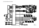
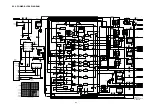
S2. BLOCK DIAGRAM

S2.1. OVERALL BLOCK DIAGRAM

IC3004

PRE PROCESS

IC3002

V-DRIVE

FOCUS

ZOOM

CDS,AGC,A/D,

TG

IC6003

SDRAM/256M-bit

SD

CARD

IC5001

AUDIO AMP

MICROPHONE AMP

MICROPHONE

DIGITAL/ AV OUT

TERMINAL

IC4001

LCD COLOR

DRIVER

(POWER SUPPLY)

DC IN/EXT. TERMINAL

BATTERY

REAR OPERATION UNIT

IC2001

VIDEO AMP

SHUTTER

IC7001

MOTOR DRIVE,

OIS DRIVE&

PRE PROCESS

FLASH

TOP OPERATION UNIT

X9101

(32.768KHz)

IC1001

POWER

IRIS

(ND)

IC9101

SYSTEM IC

IC6002

FLASH ROM/

16M-bit

X3001

(36.0MHz)

OIS

UNIT

IC3101

CCD

8.4 MEGA PIX

COLOR LCD

PANEL

2.5" PANEL

IC6001

VENUS2

CAMERA PROCESS

J-PEG COMP/EX PANDS

MEDIA I/F

USB I/F

MAIN MICROPROCESSOR

OIS CONTROL

LENS DRIVE

DMC-LX1

OVERALL BLOCK

DIAGRAM

Summary of Contents for DMCLX1PP - DIGITAL STILL CAMERA

Page 1: ...nauthorized copying and distribu tion is a violation of law ORDER NO DSC0508018CE B26 Digital Camera DMC LX1PP DMC LX1EB DMC LX1EG DMC LX1EGM DMC LX1GC DMC LX1GD DMC LX1GK DMC LX1GN DMC LX1GT DMC LX1SG Vol 1 Colour S Silver Type Except GD K Black Type Except GN GT SG ...

Page 2: ...rtant Notice 1 Other than U S A and Canadian Market 9 3 4 How to Define the Model Suffix NTSC or PAL model 10 4 Specifications 12 5 Location of Controls and Components 13 6 Service Mode 16 6 1 Error Code Memory Function 16 6 2 Confirmation of Firmware Version 19 7 Service Fixture Tools 20 7 1 Service Fixture and Tools 20 7 2 When Replacing the Main PCB 20 7 3 Service Position 21 8 Disassembly and ...

Page 3: ...exposed to shock hazards 1 2 Leakage Current Cold Check 1 Unplug the AC cord and connect a jumper between the two prongs on the plug 2 Measure the resistance value with an ohmmeter between the jumpered AC plug and each exposed metal lic cabinet part on the equipment such as screwheads connectors control shafts etc When the exposed metal lic part has a return path to the chassis the reading should ...

Page 4: ...g Procedure 1 Refer to the disassemble procedure and Remove the necessary parts unit 2 Put the insulation tube onto the lead part of Resistor ERG5SJ102 1kΩ 5W an equivalent type of resistor may be used 3 Put the resistor between both terminals of capacitor on FLASH PCB for approx 5 seconds 4 After discharging confirm that the capacitor voltage is lower than 10V using a voltmeter Fig F1 ...

Page 5: ...nly a grounded tip soldering iron to solder or unsolder ES devices 4 Use only an antistatic solder removal device Some solder removal devices not classified as antistatic ESD protected can generate electrical charge sufficient to damage ES devices 5 Do not use freon propelled chemicals These can generate electrical charges sufficient to damage ES devices 6 Do not remove a replacement ES device fro...

Page 6: ... must not be used until a replacement cover is obtained A replacement fuse cover can be purchased from your local Panasonic Dealer If the fitted moulded plug is unsuitable for the socket outlet in your home then the fuse should be removed and the plug cut off and disposed of safety There is a danger of severe electrical shock if the cut off plug is inserted into any 13 ampere socket If a new plug ...

Page 7: ...ushita Battery Industrial Co Ltd It must never be subjected to excessive heat or discharge It must therefore only be fitted in requirement designed specifically for its use Replacement batteries must be of same type and manufacture They must be fitted in the same manner and location as the original battery with the correct polarity contacts observed Do not attempt to re charge the old battery or r...

Page 8: ...8 NOTE Above caution is applicable for a battery pack which is for DMC LX1 series as well ...

Page 9: ...soldering iron with temperature control please set it to 700 20 F 370 10 C Pb free solder will tend to splash when heated too high about 1100 F 600 C When soldering or unsoldering please completely remove all of the solder on the pins or solder area and be sure to heat the sol dering points with the Pb free solder until it melts enough 3 3 Important Notice 1 Other than U S A and Canadian Market 1 ...

Page 10: ...t is the difference is that the INITIAL SETTING data which is stored in Flash ROM mounted on Main PCB 3 4 1 Defining methods To define the model suffix to be serviced refer to the nameplate which is putted on the bottom side of the Unit NOTE After replacing the MAIN PCB be sure to achieve adjustment The adjustment instruction is available at software download on the Support Information from NWBG P...

Page 11: ...n the Power off Step 5 Set the INITIAL SETTING Select the area with pressing UP DOWN of Cross key and then press the RIGHT of Cross key The only set area is displayed and then press the RIGHT of Cross key after confirmation The unit is powered off automatically Confirm the display of PLEASE SET THE CLOCK in English when the unit is turned on again Step 6 CONFIRMATION The display shows PLEASE SET T...

Page 12: ...12 4 Specifications ...

Page 13: ...13 5 Location of Controls and Components ...

Page 14: ...14 ...

Page 15: ...15 ...

Page 16: ...of factory setting Set the mode dial to P While pressing Optical Image Stabilizer Button and UP of Cross key simultaneously and hold them turn the Power on 2 The display of error code Press Optical Image Stabilizer Button MENU and LEFT of Cross key simultaneously with the step 1 condition The display is changed as shown below when the above buttons is pressed simultaneously Normal display Error co...

Page 17: ...tect error FP9001 3 5 signal line or IC6001 VENUS 2 0030 ENC1 detect error Zoom encoder detect error FP9001 5 signal line or IC6001 VENUS 2 0040 ENC2 detect error Zoom encoder detect error FP9001 3 signal line or IC6001 VENUS 2 Focus 0001 HP Low detect error Focus encoder always Low detect error FP9001 30 signal line or IC6001 VENUS 2 0002 HP High detect error Focus encoder always High detect erro...

Page 18: ...me out Communication between Lens system and IC6001 VENUS 2 0002 Camera task invalid code error IC6001 VENUS 2 0100 File time out error in recording motion image IC6001 VENUS 2 0200 File data send error in recording motion image IC6001 VENUS 2 Monitor 1000 AF frame movement check time out IC6001 VENUS 2 Operation Power on 3B00 0000 FLASHROM processing early period of camera during movement Zoom Zo...

Page 19: ...version Set the mode dial to Playback and then press DISPLAY to switch to LCD with indication Fig A Press Optical Image Stabilizer and DOWN of Cross key simultaneously No need to keep pressing The version information is displayed on the LCD with light blue colour letters Fig B CAUTION The version information does not display if the LCD has switched to LCD with indication already In this case press...

Page 20: ... are used for checking and servicing this unit 7 2 When Replacing the Main PCB After replacing the MAIN PCB be sure to achieve adjustment The adjustment instruction is available at software download on the Support Information from NWBG PAVC web site in TSN system together with Maintenance software ...

Page 21: ...igh voltage circuit on FLASH PCB 3 DO NOT allow other parts to touch the high voltage circuit on FLASH PCB No Parts No Connection Form 1 VFK1951 FP9001 MAIN LENS FPC 39PIN 0 3 FFC 2 VFK1480 FP9002 MAIN AFMF ASPECT FPC 6PIN 0 5 FFC 3 VFK1976 FP9003 MAIN LCD FPC 19PIN 0 5 FFC 4 VFK1974 FP9004 MAIN BACKLIGHT FPC 4PIN 0 5 FFC 5 VFK1950 FP9005 MAIN CCD FPC 33PIN 0 3 FFC 6 VFK1582A1225 FP9006 MAIN FP800...

Page 22: ...22 8 Disassembly and Assembly Instructions 8 1 Disassembly Flow Chart 8 2 PCB Location ...

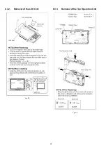
Page 23: ...ews H Jack Door unit FP9001 Flex FP9006 Flex P9001 Connector 1 Locking tab Main PCB 6 Lens Unit Fig D6 1 Locking tab Lens Unit 7 Battery Case Fig D7 1 Screw I 3 Locking tabs Strap Holder Battery Case 8 Top Operation PCB Fig D8 4 Screws J Top Operation PCB 9 Flash Unit Fig D10 1 Screw K 1 Locking tab Nut Plate Flash Unit 10 Flash PCB Fig D11 P8001 Connector P8002 Connector 2 Locking tabs Flash PCB ...

Page 24: ...24 8 3 2 Removal of the LCD Unit Fig D2 8 3 3 Removal of the Top Operation Unit Fig D3 ...

Page 25: ...25 8 3 4 Removal of the Front Case Unit Fig D4 8 3 5 Removal of the Main PCB Fig D5 8 3 6 Removal of the Lens Unit Fig D6 ...

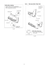
Page 26: ...26 8 3 7 Removal of the Battery Case Fig D7 8 3 8 Removal of the Top Operation PCB Fig D8 ...

Page 27: ...27 Fig D9 8 3 9 Removal of the Flash Unit Fig D10 ...

Page 28: ...28 8 3 10 Removal of the Flash PCB Fig D11 8 3 11 Removal of the Lens Ornament Unit Fig D12 8 3 12 Removal of the MF AF Aspect FPC Fig D13 ...

Page 29: ...t is install ing Disassembling procedures for the CCD unit refer to item 8 6 2 Take care that the dust and dirt are not entered into the lens In case of the dust is putted on the lens blow off them by airbrush 3 Do not touch the surface of lens 4 Use lens cleaning KIT BK VFK1900BK 5 Apply the grease VFK1829 to the point where is shown to Grease apply in the figure When the grease is applied use a ...

Page 30: ...row from lens side and then remove the unit of drive direct unit 1st lens frame 2nd lens frame move unit 3rd lens frame move unitfrom the fixed frame unit 1 Push the 1st lens frame move unit to the indicated by arrow from lens side and then remove the unit of 1st lens frame 2nd lens frame move 3rd lens frame moveunit from the drive direct unit 1 Push the 3rd lens frame move unit to the indicated b...

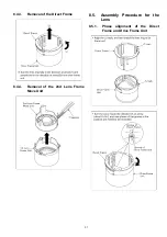
Page 31: ...31 8 4 3 Removal of the Direct Frame 8 4 4 Removal of the 2nd Lens Frame Move Unit 8 5 Assembly Procedure for the Lens 8 5 1 Phase alignment of the Direct Frame and Drive Frame Unit ...

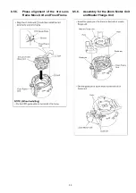
Page 32: ...32 8 5 2 Phase alignment of the Drive Direct Unit and Fixed Frame 8 5 3 Phase alignment of the 1st Lens Frame Unit and Fixed Frame 8 5 4 Phase alignment of the 2nd Lens Frame Move Unit and Fixed Frame ...

Page 33: ...33 8 5 5 Phase alignment of the 3rd Lens Frame Move Unit and Fixed Frame 8 5 6 Assembly for the Zoom Motor Unit and Master Flange Unit ...

Page 34: ...34 8 6 Removal of the CCD To prevent the CCD unit from catching the dust and dirt do not remove the CCD unit except for replacing ...

Page 35: ...nnection between the PC and this unit with USB cable 2 LCD adjustment Adjustment for LCD It need the connection between the PC and this unit with USB cable The adjustment instruction is available at Software download on the Support Information from NWBG PAVC web site in TSN System together with maintenance software 10 Maintenace 10 1 Cleanig Lens and LCD Panel Do not touch the surface of lens and ...

Page 36: ......

Page 37: ...C DMC LX1GD DMC LX1GK DMC LX1GN DMC LX1GT DMC LX1SG DSC0508018CE Diagrams and Replacement Parts List 1 Although reference number of the parts is indicated on the P C B drawing and or schematic diagrams it is NOT mounted on the P C B when it is displayed with mark 2 It is only the Test Round and no terminal Pin is available on the P C B when the TP Test Point indicated as mark 3 The voltage being i...

Page 38: ...SUPPLY DC IN EXT TERMINAL BATTERY REAR OPERATION UNIT IC2001 VIDEO AMP SHUTTER IC7001 MOTOR DRIVE OIS DRIVE PRE PROCESS FLASH TOP OPERATION UNIT X9101 32 768KHz IC1001 POWER IRIS ND IC9101 SYSTEM IC IC6002 FLASH ROM 16M bit X3001 36 0MHz OIS UNIT IC3101 CCD 8 4 MEGA PIX COLOR LCD PANEL 2 5 PANEL IC6001 VENUS2 CAMERA PROCESS J PEG COMP EX PANDS MEDIA I F USB I F MAIN MICROPROCESSOR OIS CONTROL LENS...

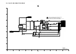
Page 39: ... 1 4 3 2 1 4 3 2 1 4 3 2 1 4 3 2 1 4 3 S9503 LEFT S9504 RIGHT S9502 DOWN S9501 UP S9506 MENU S9508 DELETE S9507 DISPLAY 13 D9501 POWER LED D3V LED0 BA1 BA0 SDBA1 SDBA0 Bank Adr DQ15 DQ0 SDD31 SDD0 A11 A0 SDA11 SDA0 CPUD31 CPUD16 DQ15 DQ0 CPUAD1 CPUAD20 A19 A0 RL9108 RL9107 RL9109 CL9502 218 215 219 KEYIN1 24 CL9505 CL9504 CL9503 CL9501 RL9106 RL9113 RL9114 CL9901 CL9913 CL9912 CL9904 CL9905 CL9906...

Page 40: ...86 185 217 AUDIO IN AUDIO SO AUDIO SCK AUDIO CS AUDIO PWM A D CONVERTER IC5001 AUDIO AMP 28 VIDEO OUT 197 VIDEO MUTE RSTB RESET DATA ADDRESS CTL SIG 180 SYSCK SDDAT1 SDDAT0 1 4 3 2 L2001 23 24 RESETOUT 3 48 1 47 IC9101 SYSTEM IC 2 SO SI SCLK SIOUT SCLK OUT LOGIC LPF ABIAS 209 QR5001 18 ALC 19 23 EVR 4 1 D D S 5 1 D D S 99 100 JK2001 DIGITAL AV OUT TERMINAL VIDEO OUT 2 LINE OUT 3 USB 5 USB 7 USB CA...

Page 41: ...Unit pixels OB AREA TRANJENT AREA EFFECTIVE AREA FP9005 23 22 21 OV4 20 OV5A 61 46 51 VB V6 H1 H2 HL RG FP9005 9 FP9005 10 FP9005 11 FP9005 14 FP9005 15 FP9005 16 9 V2 6 V3A 5 V3B 4 V4 3 V5A 2 V5B CL3013 CL3012 RL3009 RL3008 RL3007 FLASH TRG CCDVD CCDHD CCD IN X3001 36 0MHz CLI 24 CLO 23 1 2 33 4 SUBCNT 3 55 26 30 OV5B OV5R VH Q3102 FP9005 7 11 V1A 8 7 FP9005 12 FP9005 13 FP9005 18 FP9005 19 25 V7...

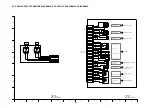
Page 42: ...P9001 21 PS9901 21 6 5 7 2 3 1 8 GYRO Y 240 GYRO SW 4 OUT VREF 1 4 OUT VREF 1 AMP AMN XINN XINP 2 IC7101 GYRO Y IC7102 GYRO X FZHP 38 37 CL9042 CL9041 CL8004 CL8009 UNREG RL9104 RL9103 CL9019 CL9018 2 1 4 3 T W CL9059 IC7103 GYRO AMP DAC LOGIC H BRIDGE CONSTANT CURRENT DRIVER 21 SYSCK DAC DAC 36 37 38 35 XFIL YDA XDA YFIL HALL AMP ADC 51 50 YINN YINP HALL AMP 16 17 19 21 18 20 14 15 12 22 13 23 XV...

Page 43: ...11 12 13 14 1 B T S 4 3 2 B T S 6 5 B T S 7 B T S 1 2 1 L E S D U 3 L E S D U 42 To 1 h c 2 h c To 3 h c To Control Block Q1101 QR1103 196 PP9001 22 PS9901 22 PP9001 21 PS9901 21 POWER SW QR1101 1 2 3 4 5 D S G Q1070 1 2 3 4 5 D S G Q1050 1 2 3 4 5 D S G Q1020 2 1 4 D1101 PGND 2 VREF GND KS UDSEL12 UDSEL3 CL1108 CL1107 CL2004 CL1101 D3V TOP OPERATION P C B OFF ON CL9904 IC6002 FLASH ROM 16Mbit 12 ...

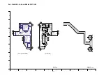
Page 44: ...D N G 1 D R A U G T U O D C C 1 0 2 6 V 2 A 3 V 3 4 V 0 1 8 V A 5 V 5 1 D C C O M R E H T 6 1 A 1 V B 1 V 2 V FP9005 2 2 R 3 2 L H 4 2 1 H 5 2 2 H 6 2 D C C D N G 7 2 B U S B 8 2 B U S 9 2 L V 0 3 H V 1 3 D C C D N G 2 3 D C C D N G 3 3 N O C K H C 6 7 8 9 1 2 4 5 A GND UNREG GND UNREG UNREG NC STROBE TRG 12 11 UNREG GND 10 FRAME GND 3 STB PWM OUT STB CHG LV 5V NC FP9006 6 7 8 9 1 2 4 5 A GND UNRE...

Page 45: ...L9910 CL9908 CL9912 CL9913 CL9905 CL9904 CL9901 CL9902 CL9917 R9901 2400 R9903 8200 R9902 4300 R9909 R9910 R9904 24K R9905 2400 R9906 4300 R9907 8200 0 R9908 L0FZBA000004 M9901 6 7 5 9 13 10 12 11 14 15 8 1 3 4 2 25 28 30 29 26 27 21 22 18 16 17 20 19 24 23 K1KB30AA0116 PS9901 1 2 3 4 S9904 ESE23J101 1 3 2 4 K0F111A00472 S9905 C C 1 2 3 12 11 16 13 14 6 15 4 5 10 9 8 7 S9901 K0G199A00010 K5H2022A0...

Page 46: ... 1M 36 68 R8004 R8021 15K 0 R8005 100K 18 R8002 CL8005 CL8010 CL8008 CL8004 CL8009 CL8001 CL8021 CL8020 CL8011 CL8003 C8004 36 F1K2J102A010 F1K0J1060025 C8009 C8007 0 1 36 C8006 F1K2E4730002 F1H0J1060002 C8001 B0HCMP000006 D8002 B0HCGV000002 D8003 3 4 1 2 8 7 5 6 B1JBLP000008 Q8001 1 8 6 4 2 3 5 7 9 11 12 10 FP8001 K1MN12BA0051 3 2 1 4 5 6 Q8009 B1DFCG000010 K5H122200007 F8001 1 3 2 4 G5D1A0000038...

Page 47: ...ND 24 SHUT 1 25 SHUT 1 26 SHUT 2 27 SHUT 2 28 D3V 29 FZHP 30 FZHP LED 31 FMBN 32 FMAN 33 FMBP 34 FMAP 35 IRIS 3 36 IRIS 4 37 IRIS 2 38 IRIS 1 39 ZENC1 LED 4 ZENC2 3 ZENC2 LED 2 D3V 1 COIL PHOTO SENSOR ZOOM ENCODER 2 PHOTO SENSOR ZOOM ENCODER 1 DRIVE COIL Y DRIVE COIL X HALL SENSOR X HALL SENSOR Y OIS UNIT CO BARREL ENCODER FULL RETRACT DC SOLENOID IRIS SHUTTER UNIT IRIS H1 H2 H3 D11 D12 E1 E2 D10 ...

Page 48: ...01 2SC4627J0L Q3102 1 2 4 6 8 9 7 5 3 32 33 28 26 27 31 29 30 23 24 21 11 10 18 17 20 19 13 12 16 14 15 22 25 MAINCN ERTJ0EG103HA TH3101 V5A V5A V5B V5B V3A V3A V4 V4 V3B V3B V2 V2 V1B V1B V7A V7A V8 V8 V7B V7B V6 V6 V1A V1A V5R V5R V7R V7R R H2 H2 H1 H1 V7R V7R V5R V5R NC NC NC NC NC NC NC HL HL V3B V3B V4 V4 V7A V7A V7B V7B V5A V5A V5B V5B V6 V6 V3A V3A V8 V8 V1A V1A GND GND V1B V1B PT VDD VO RG...

Page 49: ...9 0 1 3 2 1 J K 9 9 0 1 F 9 9 0 1 C L 9 9 1 1 C L 9 9 1 0 C L 9 9 0 9 C L 9 9 0 8 C L 9 9 0 7 6 5 4 3 2 1 S9906 4 3 2 1 S9905 2 1 3 4 S9904 6 5 4 3 2 1 S9903 6 5 4 3 2 1 S9902 15 16 12 11 14 13 5 4 3 1 10 9 8 7 6 2 S9901 R9910 R9909 R9908 R9907 R9906 R9905 R9904 R9903 R9902 R9901 1 2 M9901 1 1 ET9902 1 1 ET9901 CL9917 CL9916 CL9915 CL9914 CL9913 CL9912 CL9906 CL9905 CL9904 CL9903 CL9902 CL9901 S4 ...

Page 50: ...4 3 2 1 T 8 0 0 1 R 8 0 0 6 1 2 P 8 0 0 2 1 2 P 8 0 0 1 D 8 0 0 3 D 8 0 0 2 C L 8 0 0 1 C 8 0 0 4 C 8 0 0 3 R8033 R8032 R8021 R8013 R8005 R8004 R8003 R8002 1 2 3 4 5 6 Q8009 1 2 3 4 5 6 7 8 Q8001 1 2 3 4 5 IC8001 10 5 1 12 FP8001 F8001 CL8021 CL8020 CL8011 CL8010 CL8009 CL8008 CL8005 CL8004 CL8003 C8009 C8007 C8006 C8001 4 3 2 1 S9802 4 3 2 1 S9801 ...

Page 51: ...R3105 R3103 R3102 R3101 Q3102 Q3101 32 31 30 25 20 17 16 15 14 10 5 1 IC3101 C3103 C3101 SHUTTER UNIT SHUTTER D6 D5 D4 D3 D2 D1 E Pin 39 Pin 1 OIS UNIT D A1 A3 A2 B1 B2 B3 ZOOM ENCODER 2 A ZOOM ENCODER 1 B C2 ZOOM MOTOR UNIT C C1 D7 D8 D9 D10 D11 D12 E2 E1 H4 H3 H2 H1 G4 G3 G2 G1 F1 F2 F3 SHUTTER UNIT IRIS H FOCUS MOTOR UNIT G CO BARREL ENCODER FULL RETRACT F ...

Page 52: ...S 16 ...

Page 53: ...ent parts according to this list 2 IMPORTANT SAFETY NOTICE Components identified with the mark have the special characteristics for safety When replacing any of these components use only the same type 3 Unless otherwise specified All resistors are in OHMS K 1 000 OHMS All capacitors are in MICRO FARADS uf P uuF 4 The P C Board units marked width show below the main assembled parts 5 The marking RT...

Page 54: ...SC4627JCL TRANSISTOR 1 Q3102 2SC4627JCL TRANSISTOR 1 JK9901 K4ZZ03000323 CONNECTOR BATT 3P 1 R3101 ERJ2GEJ100 M RESISTOR CH 1 16W 10 1 PS9901 K1KB30AA0116 CONNECTOR 30P 1 R3102 ERJ2GEJ222 M RESISTOR CH 1 16W 2 2K 1 R3103 ERJ2GEJ183 M RESISTOR CH 1 16W 18K 1 R9901 ERJ2GEJ242 M RESISTOR CH 1 16W 2 4K 1 R3105 ERJ2RKD330 M RESISTOR CH 1 16W 33 1 R9902 ERJ2GEJ432 M RESISTOR CH 1 16W 4 3K 1 ERJ2GEJ432X ...

Page 55: ...11 VHD1678 SCREW 1 SILVER 15 VYK1T59 FRONT CASE ASS Y 1 SILVER B11 VHD1813 SCREW 1 BLACK 15 VYK1T60 FRONT CASE ASS Y 1 BLACK B12 VHD1678 SCREW 1 SILVER 16 VWJ1802 FPC 1 B12 VHD1813 SCREW 1 BLACK 17 VGQ8519 COUPLING PLATE 1 B13 VHD1678 SCREW 1 SILVER 18 VYK1Q49 LENS ORNAMENT UNIT 1 B13 VHD1813 SCREW 1 BLACK 19 VEP59019A ASPECT C B A 1 RTL B14 VHD1678 SCREW 1 SILVER 20 VGL1169 REAR PANEL LIGHT 1 B14...

Page 56: ...VXP2557 1ST LENS FRAME UNIT 1 SILVER 117 VXP2509 1ST LENS FRAME UNIT 1 BLACK 118 VXP2510 2ND LENS FRAME UNIT 1 119 VXP2517 3RD LENS FRAME UNIT 1 121 VDW1187 LENS RING FRONT 1 122 VXP2558 DRIVE FRAME UNIT 1 SILVER 122 VXP2518 DRIVE FRAME UNIT 1 BLACK 125 VXQ1355 FIX FRAME UNIT 1 126 VXQ1356 MASTER FRANGE UNIT 1 127 VXW0772 LENS U 1 SILVER 127 VXW0732 LENS U 1 BLACK B110 VHD1726 SCREW 1 B111 VHD1726...

Page 57: ... VQT0S22 INSTRUCTION BOOK 1 EGS EGK 213 VQT0U21 O I SOFTWARE 1 GTS GERMAN CHINESE TRADITIONAL 210 VQT0S23 INSTRUCTION BOOK 1 EGS EGK 214 VYQ3509 BATTERY PROTECTION CASE U 1 FRENCH 215 RP SD032BVE0 SD CARD 32MB 1 210 VQT0S24 INSTRUCTION BOOK 1 EGS EGK 216 VPK3035 PACKING CASE 1 PPS ITALIAN 216 VPK3039 PACKING CASE 1 PPK 210 VQT0S25 INSTRUCTION BOOK 1 EGS EGK 216 VPK3036 PACKING CASE 1 EBS EGS EGMS ...

Page 58: ...1 FRAME CASING SECTION 1 S 22 18 B27 B26 19 B12 B13 15 B6 B25 B24 B19 B10 B11 29 B20 32 C8003 16 31 30 3 B22 8 B5 12 4 5 14 B3 6 7 B23 9 2 1 B21 4 B2 11 10 B4 B1 27 28 25 13 17 26 B18 B16 B15 B17 33 B8 B9 23 20 B7 B14 24 22 ...

Page 59: ...S6 2 FRAME CASING SECTION 2 S 23 121 122 125 B113 B114 117 118 119 B120 116 B119 B118 B117 B116 111 112 126 B115 110 113 103 B112 B110 B111 115 116 2 116 1 127 ...

Page 60: ...CKING PARTS ACCESSORIES SECTION S 24 204 205 216 223 224 202 203 206 209 213 210 212 201 214 225 208 215 207 DMC LX1GN DMC LX1GK DMC LX1EB GC SG DMC LX1EG EGM GC SG DMC LX1GD 220 DMC LX1GT 222 217 218 219 221 ...

Reviews: