background image

RECEIVER

Issue 1

Section 5

MCUK991001G8

Revision 0

– 16 –

Technical Guide

5.3 Functional Description

5.3.1 Dual Band Receiver IC

The main building block for the Dual Band Receiver is the Hitachi Bright2 IC. The receiver is a triple superheterodyne type with 
the 1st IF at 225 MHz and 2nd IF at 45 MHz. The intermediate frequencies are common to both frequency bands.

The Rx IC contains the following stages:

1.

Gain controlled 1st mixer for GSM 900 band.

2.

Gain controlled 1st mixer for GSM 1800 band.

3.

Gain controlled 2nd mixer.

4.

Gain controlled IF amplifier

5.

I,Q quadrature down converter.

6.

Baseband Op Amps for further amplification and some filtering of the baseband I,Q signals.

5.3.2 Circuit Description

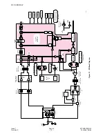
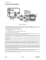
Figure 5.1:  Dual Band Receiver

RF input to the receiver is either via the antenna or via the H/F RF connector. The input signal from the antenna or the H/F RF 
connector is fed into the GSM 900/GSM 1800 dual band Antenna switch module which comprises a diplexer and diode 
switches. The diplexer splits the two GSM frequency bands whilst the pin switches route the signal flow from the receiver and 
the transmitter as required. 
The output is applied to the 1st dual band receiver SAW filter which provides the roofing filter for the Rx front end for both 
900 MHz and 1800 MHz bands. Note that the appropriate signal path will be set by the Antenna switch module.
The dual band LNA IC requires external matching in order to achieve a fixed gain of 17 dB (GSM 900) or 16dB (GSM 1800), 
a typical noise factor of 1.7 dB on either band, and a third order intercept point at its input of -8 dBm (GSM 900) or -5 dBm 
(GSM 1800).
The output from the LNA passes through a second dual band SAW filter before being matched differentially into the 1st down-
converter mixer of the Bright 2 dual band receiver IC. The gain of the 1st mixer stage can be reduced from, typically, 9 dB to  
-2.5 dB (GSM 900) or 8.5 dB to -3.5 dB (GSM 1800); this is required for operation under strong signal conditions where input 
power levels are greater than -40 dBm.
The mixer has a minimum third order input intercept point of 2 dBm (GSM 900) or -0.5 dB (GSM 1800) with a maximum SSB 
noise figure of 12 dBm (GSM 900) or 10.6 dB (GSM 1800). The 1st local oscillator output is generated by a PLL employing a 
dual modular RF VCO. The output from the VCO is split and fed directly to the Bright 2, which then buffers the signal and 
differentially splits this to both 900 MHz and 1800 MHz mixers. The frequency range of the local oscillator for GSM 900 is 1160-
1185 MHz, and for GSM 1800 is 1580-1655 MHz.
The IF output at 225 MHz from the 1st mixer is filtered by the differential IF SAW filter before it is fed into the 2nd mixer and 
down-converted to the 2nd IF of 45 MHz. The output is then fed to the gain-controlled IF amplifiers
The output from the IF amplifiers is fed into two quadrature mixers where it is converted down to baseband. The IF LO is 
generated at 540 MHz by an external discrete VCO module. An on-chip divider on the Rx IC divides this by twelve. It also 
produces two outputs in quadrature to generate the baseband I and Q signals. The outputs from the mixers are connected to 
external pins via dual differential low pass filters and a pair of buffer amplifiers.

DUAL BAND

LNA

PGC

1800

DUAL BAND

RX SAW

DUAL BAND RECEIVER 

(PART)

IF

SAW

1st

Mixer

2nd

Mixer

900

1800

900

LPF

Rx

Tx

Rx

Tx

Ext

Ant.

HPF

10154-1

DUAL BAND

Rx SAW

S701

I

Q

Demodulator

U701

S700

FL702

U700

FL703

DIPLEXER

FL700

Summary of Contents for EB-GD30

Page 1: ...0 130 g with EB BSD30 Battery 170 g with EB BLD30 GD50 115 g with EB BSD50 Battery 170 g with EB BLD30 Display Graphical chip on glass liquid crystal Alphanumeric 16 x 3 characters 5 icons and 6 x 1 c...

Page 2: ...ustrial UK Ltd accepts no responsibility for inaccuracies which may occur and reserves the right to make changes to specification or design without prior notice The information contained in this manua...

Page 3: ...r 12 4 TRANSMITTER 4 1 Introduction 13 4 2 Uplink Frequencies 13 4 3 Functional Description 14 5 RECEIVER 5 1 Introduction 15 5 2 Downlink Frequencies 15 5 3 Functional Description 16 6 BASEBAND OVERV...

Page 4: ...Issue 1 Section MCUK991001G8 Revision 0 iv Technical Guide This page is left intentionally blank...

Page 5: ...talling operating and servicing e g disassembly and testing the telephone system are provided in the associated Service Manual 1 2 Structure of the Guide The guide is structured to provide service eng...

Page 6: ...INTRODUCTION Issue 1 Section 1 MCUK991001G8 Revision 0 2 Technical Guide This page is left intentionally blank...

Page 7: ...133 17 KBC 2 Key Column 2 signal for Key scan GEMINI pin 130 18 KBC 3 Key Column 3 signal for Key scan GEMINI pin 129 19 KBC 4 Key Column 4 signal for Key scan GEMINI pin 128 20 KBR 0 Key Row 0 signal...

Page 8: ...y sleep mode and therefore minimise the drain on the car battery nLOGIC_POWER Hi Z H Normal mode 2 Satisfy 2nd of 2 conditions for sending initialise Testset command and entering Testset mode see nADP...

Page 9: ...or 2nd condition H MH Condition 1 satisfied M ML L Enter Testset Mode not satisfied 15 NH F_ON 1 Accessory Sending Receiving Audio paths unmute L unmute Hi Z mute 16 GND 6 Refer to pin 1 Refer to pin...

Page 10: ...Determine whether a battery is attached to the H H 2 Monitor battery temperature for the purposes of charging H Abnormal battery M Li or NiMH charging L No battery or abnormal battery 3 GND 1 Negative...

Page 11: ...KBC 2 TP13B SSDR U504 pin 19 TP14 KBC 3 TP14B RYnBY U502 pin 16 TP15 KBC 4 TP15B RnW TP16 nPOWKEY TP17 CHLEDOUT TP17B GROUND TP18 PGLEDOUT TP18B DSP INT U503 pin 94 TP19 BKLTOUT TP19B TDO_BSCAN U503...

Page 12: ...ide 2 2 2 Keypad PCB TP No Signal TP1 EAR_P TP2 EAR_N TP3 DS12 TP4 DS11 TP5 DS10 TP6 DS9 TP7 DS8 TP8 DS7 TP9 DS6 TP10 DS5 TP11 DS4 TP12 DS3 TP13 DS2 TP14 DS1 TP15 CH LEDOUT TP16 PG LEDOUT TP17 BKLT OU...

Page 13: ...in line connector A metallised plastic chassis is used to separate the Main and the Keypad PCBs When the chassis is sandwiched between the Main and the Keypad PCBs the groundplane of the Main board t...

Page 14: ...85MHz DCS 1580 1655MHz 45MHz GSM 890 915MHz DCS 1710 1785MHz ANT GSM LNA DCS LNA DCS DUAL PLL IC PGC Gain TXON1 RXON1 RXON2 IF VCO 10152 1 DIPLEXER GSM DUAL RF VCO DUAL Rx SAW FILTER DUAL LNA IC GN010...

Page 15: ...d to 520 MHz For this choice of IF no transmitter in band spurious is believed to occur due to harmonics of the 1st LO The third local oscillator runs at 45 MHz to mix the 2nd IF down to baseband It s...

Page 16: ...ch contains a micro switch If the switch is open the RF signal is routed to the hands free unit If it closed the signal is routed back via the Main PCB to the antenna This routing of the RF signal up...

Page 17: ...91 600 892 600 893 600 894 600 890 800 891 800 892 800 893 800 894 800 891 000 892 000 893 000 894 000 895 000 26 30 31 35 36 40 41 45 46 50 895 200 896 200 897 200 898 200 899 200 895 400 896 400 897...

Page 18: ...to any required level up to PL5 33 dBm at the antenna for GSM 900 and PL0 30 dBm for GSM 1800 PA output is applied to the antenna via a low pass filter to remove unwanted harmonics The coupled outputs...

Page 19: ...00 937 600 938 600 939 600 935 800 936 800 937 800 938 800 939 800 936 000 937 000 938 000 939 000 940 000 26 30 31 35 36 40 41 45 46 50 940 200 941 200 942 200 943 200 944 200 940 400 941 400 942 400...

Page 20: ...ut from the LNA passes through a second dual band SAW filter before being matched differentially into the 1st down converter mixer of the Bright 2 dual band receiver IC The gain of the 1st mixer stage...

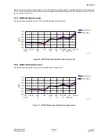
Page 21: ...hrough the receiver IC for the GSM 900 band are given below Figure 5 2 GSM 900 Nominal and Worst Case Signal Levels 5 3 4 GSM 1800 Signal Levels The signal levels through the receiver IC for the GSM 1...

Page 22: ...RECEIVER Issue 1 Section 5 MCUK991001G8 Revision 0 18 Technical Guide This page is left intentionally blank...

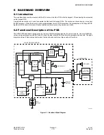
Page 23: ...ting spurious emissions 6 2 Functional Description of the PCB The GD30 GD50 baseband is based around a two chip GSM chipset developed by Texas Instruments One chip GEMINI carries out signal processing...

Page 24: ...able to support 5 V tolerant inputs Therefore in order to Interface GEMINI with a 2 8 V supply and the SIM with a 5 V supply it is necessary to include a level shift U501 is able to perform the requir...

Page 25: ...sing Unit TPU The TPU provides the GSM TDMA timing requirements for the system external timing signals are provided by an area of Microcode within the GEMINI chip 6 2 5 CPU Memory GD30 GD50 uses a Dua...

Page 26: ...battery is removed a small rechargeable back up battery VBACKUP is used This power source also provides power back up for data held in the SRAM The RTC can be calibrated using a high precision oscill...

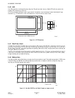
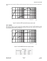
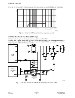
Page 27: ...ply a low impedance dynamic speaker must be used The GSM standard requires that the receive audio frequency response in Handheld use must fit within the mask shown below GD30 and GD50 is designed to m...

Page 28: ...riven by the ear piece amplifier inside VEGA U504 GD50 can operate in desktop internal hands free mode This is achieved by disabling the ear piece amplifier and driving the speaker from the auxiliary...

Page 29: ...ither as auto reload or one shot timers to provide interrupts to the ARM CPU A prescaler and 16 bit register define the timer clock duration The Timer unit receives a 928 kHz clock signal from the GEM...

Page 30: ...BASEBAND OVERVIEW Issue 1 Section 6 MCUK991001G8 Revision 0 26 Technical Guide This page is left intentionally blank...

Page 31: ...e software 7 2 2 CPU The CPU is an ARM7 32 bit RISC micro controller core It can work in 32 or 16 bit instruction modes and on 32 16 or 8 bit data Pipelining is employed so that all parts of the proce...

Page 32: ...CPU DSP shared ram 16 bits APIC 0050 4000 1k CPU DSP interface controller 16 bits TPU RAM 0050 4400 1k GSM timer Micro code RAM 16 bits SIM 0050 4800 1k SIM interface 16 bits TSP 0050 4C00 1k Timed S...

Page 33: ...tion I O IO 0 nLCDCS 117 nPULSE Watchdog Timer Pulse High Pulse _ _ 500 ns min O I O 1 RXE 116 LOGIC_PWR 1 PSU kept on 0 PSU off O I O 2 TXE 112 nEXT_PWR 1 External Power Supply 0 Battery Power Supply...

Page 34: ...GEMINI Issue 1 Section 7 MCUK991001G8 Revision 0 30 Technical Guide This page is left intentionally blank...

Page 35: ...ture of the baseband uplink path TIMING JTAG BURST STORE GMSK MOD FILTER FILTER DSP INTERFACE 10 bit I DAC 8 bit SIGMA DELTA RAMP DATA SIGMA DELTA 10 bit DAC SP INTERFACE 10 bit Q DAC 8 bit DAC 8 bit...

Page 36: ...ristics The ramp time is selectable between each step being 1 16 of a bit and each step being 1 8 of a bit giving a maximum ramp time of either 14 77 s or 29 53 s An 8 bit value is used to program the...

Page 37: ...e for the digital audio samples processed by the DSP in GEMINI Voice Uplink Path Figure 8 6 Voice ADC block diagram RINT1 RINT2 VTCXO CEXT AFC 3 5V 13 BIT DIGITAL MODULATOR 1 BIT DAC LOW PASS FILTER P...

Page 38: ...ctrical volume for calibration of this DAC VEGA input Pin Number Use Range ADIN1 36 Battery Voltage BAT_VOLT 000h 0V 3FFh 5 5 V ADIN2 37 Battery ID BAT_ID 000h 135h Ni MH 136h 3FFh Li Li polymer ADIN3...

Page 39: ...procedure has two phases If an initial check to see if the battery is in good condition is successful the second phase determines the source of the power up request key press external power accessory...

Page 40: ...ed functionality e g from active to charge mode When the new mode is OFF or sleep the CPU will set STAY_ALIVE LOW Battery Condition HF nEXT_PWR nIGNITION KBR0 LOGIC_PWR Mode OK X X X 1 1 active LOW X...

Page 41: ...ry Charging Monitoring 5 Accessory Control The power amplifiers used in GD30 GD50 are powered directly from the battery supply to maximise the power available to them They operate at full specificatio...

Page 42: ...GEMINI U503 nRESET 13MHz 2V8 1V8 VDSP VBAT 2V8 EXT_PWR PA ON ADCON CHARGE_ON VSET CURRENT BAT_VOLT CHARGING ASIC MCU SERIAL INTERFACE nON_HOOK nHF_ON nHF_ON nLOGIC_PWR nHF_SENSE IGNITION nADP_SENSE O...

Page 43: ...Clock to become stable Allow reset of GEMINI and VEGA internal blocks 6 Set nRESET HIGH causing the ARM processor to start from address 0 9 5 4 Power Source Failure The SIM card contains EEPROM If th...

Page 44: ...s high 9 5 6 Battery Charging Monitoring The status of the LCD battery icon is determined by the value of BAT_VOLT returned from VEGA the battery ICON has four states The battery charging is controlle...

Page 45: ...X Low High Low yes yes yes H F Low Low Low Mid X no no no H F SMS High X Low Mid High yes no yes H F SMS High X Low Mid Low yes yes yes H F SMS Low Low Low Mid l X no no no H F PC High X Low Mid l Hi...

Reviews: