POWER SUPPLIES
MCUK991001G8
Section 9
Issue 1
Technical Guide
– 39 –
Revision 0
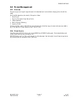
9.5.3 Power On/Off Control
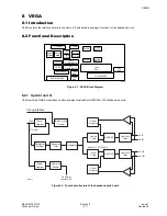
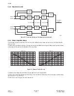
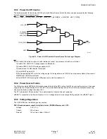
The hardware model for the Power On/Off Control and Power Source Failure functions can be expressed by the following
boolean expression and logic diagram.
On/Off = VBAT + (LOGIC_PWR · RTC_INT · (nL (nPOWKEY · nIGNITION · nEXT_PWR)))
Figure 9.2: Power On/Off Control & Power Source Failure Logic Diagram
On/Off: Initially this active low signal is under Hardware control, the purposes of which are as follows:
1) Enable 2V8, A2V8 & 2V5 voltage supplies to Baseband.
2) Enable VSRF & VSVCXO voltage supplies to RF.
3) Generation of 13 MHz Master Clock signal.
4) Set nRESET signal LOW.
5) Wait approximately 200 ms for the voltage output of the regulators and 13 MHz Clock to become stable. Allow reset of
GEMINI and VEGA internal blocks.
6) Set nRESET HIGH causing the ARM processor to start from address 0.
9.5.4 Power Source Failure
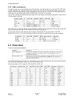
The SIM card contains EEPROM. If the battery power fails while the SIM is active, the SIM may corrupt its memory as the power
supply drops out of specification.The nLVA_INT is a non-maskable interrupt to the CPU which forces exception processing
whenever the battery voltage falls below 2.8 V.
The RTC also detects if Back-up fails. This is determined by Gemini at the next power-up.
nRESET is connected to the Gemini reset pin. A 2.4 V voltage detector in the charge ASIC generates the nRESET signal.
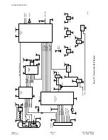
9.5.5 Voltage Regulation
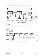
The GD30/GD50 has the following power sources:
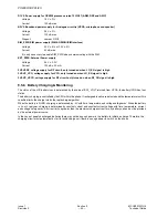
D2V8: Baseband power supply for digital circuitry (GEMINI, Memory and LCD)
Voltage:
2.8 V ± 3 %
Current:
300 mA max.
Dropout:
100 mV max. (load = 200mA)
nLVA_INT
On/Off
nPOWKEY
nIGNITION
nEXT_PWR
LOGIC_PWR
VBAT
10149-1


