


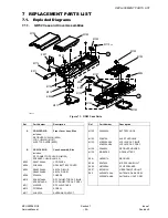


R
E
P
L
A
C
E
M
E
N
T
P
A
R
T
S
L
IS
T
M
C
U
K
0
0
0
6
0
1
C
8
S
e
c
tio
n
Is
s
u
e
1
S
e
rv
ic
e
M
a
n
u
a
l
–
6
3
–
R
e
v
is
io
n
0
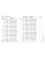
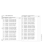
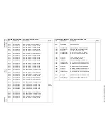
D609
MAZT068H0L
DIODE MAZT068H0L ZENER 6.8V SM
D610
MAZT068H0L
DIODE MAZT068H0L ZENER 6.8V SM
D612
MAZS0750ML
DIODE MAZS0750ML ZENER 7.5V SM
D613
MAZS0750ML
DIODE MAZS0750ML ZENER 7.5V SM
D614
B0JCDD000001
DIODE RB521S-30 SCHOTTKY 30V 2
D615
MAZT068H0L
DIODE MAZT068H0L ZENER 6.8V SM
D616
MAZT068H0L
DIODE MAZT068H0L ZENER 6.8V SM
D618
MAZS0470GL
DIODE MAZS0470G ZENER 4.7V SMD
D619
MA2S11100L
DIODE MA2S111 80V 100mA SMD SS
D620
MAZS0470GL
DIODE MAZS0470G ZENER 4.7V SMD
D621
MAZS0470GL
DIODE MAZS0470G ZENER 4.7V SMD
D625
B0JCDD000001
DIODE RB521S-30 SCHOTTKY 30V 2
DS603
LNJ115W8PRA
DIODE LED GREEN/RED 10mA SMD 1
DS604
B3ABB0000035
DIODE LED GREEN 2.2V 20mA SMD
DS605
B3ABB0000035
DIODE LED GREEN 2.2V 20mA SMD
DS606
B3ABB0000035
DIODE LED GREEN 2.2V 20mA SMD
DS607
B3ABB0000035
DIODE LED GREEN 2.2V 20mA SMD
E101
B9Z000000018
COUPLER 897.5 MHz SMD 2012 6PI
E102
EHFFD1729
COUPLER 1.747 GHz SMD 2012 6PI
FL101
EXCML16A270U
SUPPRESSOR EMI 27 OHM 4A SMD 1
FL102
EXCML16A270U
SUPPRESSOR EMI 27 OHM 4A SMD 1
FL201
EFCH9418MTYF
FILTER SAW RX GSM/PCN SMD
FL202
J0E1847B0002
FILTER DUAL LC RX SMD
FL203
EFCH225MDQA2
FILTER IF SAW 225MHz SMD
J601
JC76001A
CONNECTOR AUDIO JACK SKT 2.5mm
Model EB-GD52
Name: GD52 Main PCB
Ref
Part Number
Description
Notes
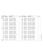
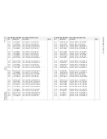
L101
ELJRE5N6JF2
INDUCTOR 5.6nH 5% SMD 1608
L102
G1C3N9Z00004
INDUCTOR 3.9nH +/-0.3nH SMD 10
L104
G1C33NJ00009
INDUCTOR 33nH 5% SMD 1005
L105
ELJRE5N6JF2
INDUCTOR 5.6nH 5% SMD 1608
L108
G1C10NJ00008
INDUCTOR 10nH 5% SMD 1005
L109
G1C5N6Z00005
INDUCTOR 5.6nH +/-0.3nH SMD 10
L151
G1C5N6Z00005
INDUCTOR 5.6nH +/-0.3nH SMD 10
L152
G1C15NJ00008
INDUCTOR 15nH 5% SMD 1005
L201
G1C10NJ00008
INDUCTOR 10nH 5% SMD 1005
L203
G1C2N7Z00007
INDUCTOR 2.7nH +/-0.3nH SMD 10
L204
G1C8N2J00004
INDUCTOR 8.2nH 5% SMD 1005
L205
G1C6N8J00004
INDUCTOR 6.8nH 5% SMD 1005
L206
G1C5N6Z00005
INDUCTOR 5.6nH +/-0.3nH SMD 10
L208
G1C5N6Z00005
INDUCTOR 5.6nH +/-0.3nH SMD 10
L209
G1C82NJ00010
INDUCTOR 82nH 5% SMD 1005
L210
G1C82NJ00010
INDUCTOR 82nH 5% SMD 1005
L211
G1CR22J00006
INDUCTOR 220nH 5% SMD 1608
L212
ELJRE56NJF3
INDUCTOR 56nH 5% SMD 1608
L213
ELJRER12JF3
INDUCTOR 120nH 5% SMD 1608
L214
G1CR10J00010
INDUCTOR 100nH 5% SMD 1005
L215
G1C3N3Z00005
INDUCTOR 3.3nH +/-0.3nH SMD 10
L217
G1C15NJ00008
INDUCTOR 15nH 5% SMD 1005
L218
ELJRE82NJF3
INDUCTOR 82nH 5% SMD 1608
L219
G1CR18J00004
INDUCTOR 180nH 5% SMD 1608
L220
ELJRER12JF3
INDUCTOR 120nH 5% SMD 1608
L303
G1C39NJ00009
INDUCTOR 39nH 5% SMD 1005
Model EB-GD52
Name: GD52 Main PCB
Ref
Part Number
Description
Notes
Summary of Contents for EB-GD52
Page 4: ...Issue 1 iv MCUK000601C8 Revision 0 Service Manual This page is left intentionally blank ...
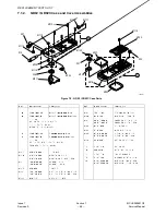
Page 83: ... 5 8 7 5 06 0 8 6HFWLRQ VVXH 6HUYLFH 0DQXDO 5HYLVLRQ H SDG 3 ...
Page 84: ... 5 8 7 5 06 VVXH 6HFWLRQ 0 8 5HYLVLRQ 6HUYLFH 0DQXDO 7KLV SDJH LV LQWHQWLRQDOO EODQN ...
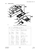
Page 87: ... 5 8 7 5 06 0 8 6HFWLRQ VVXH 6HUYLFH 0DQXDO 5HYLVLRQ H SDG 3 ...
Page 88: ... 5 8 7 5 06 VVXH 6HFWLRQ 0 8 5HYLVLRQ 6HUYLFH 0DQXDO 7KLV SDJH LV LQWHQWLRQDOO EODQN ...