background image

CALIBRATION PROCEDURES

MMCD021001C8

Section 8

Issue B

Service Manual

– 37 –

Revision 0

PROVISIONAL INFORMA

TION

GSM 1900

The following table shows the measurement limits according to power level:

The values in these tables are required only if manual Tx Trim is used to trim individual channels.

8.2.2

Automatic Calibration Procedure

This procedure requires the use of a Gigatronics 8541C power meter.

1.

Connect the test equipment as shown in Figure 6.5:

2.

Select GD87 and then select the required band, e.g. ‘GSM (900 MHz)’.

3.

With the CB2000 software running, select ‘

TX CAL’

 button  

4.

When the Tx Calibration screen is displayed, start automatic calibration by selecting the 

‘Run Auto Cal’ 

button.

5.

Once the automatic calibration has finished, select the 

‘Run Auto Verify’ 

button to verify the calibration.

6.

When finished,  select the

 ‘EXIT’

 button to save data to the handset. A confirmation message will be displayed in the next 

box.

Power Level

(PL)

Output Power (dBm)

Nominal

Target

Min

Max

0

29.25

29.0

29.5

1

28.0

27.5

28.5

2

26.0

25.5

26.5

3

24.0

23.5

24.5

4

22.0

21.5

22.5

5

20.0

19.5

20.5

6

18.0

17.5

18.5

7

16.0

15.5

16.5

8

14.0

13.5

14.5

9

12.0

11.5

12.5

10

10.0

9.5

10.5

11

8.0

7.5

8.5

12

6.0

5.5

6.5

13

4.0

3.5

4.5

14

2.0

1.5

2.5

15

0.0

-0.5

0.5

NOTE: To ensure that the telephone operates within set SAR margins, Panasonic recommends that a power meter

capable of measurement to an accuracy of ±0.2 dB is used when calibrating power levels. Use of a less
accurate power meter may result in the telephone failing to meet SAR standards. 

Summary of Contents for EB-GD87

Page 1: ...n speed 270 833 kbps Signal Reception Direct conversion Antenna Impedance 50 External Connector Antenna VSWR 2 1 1 Dimensions Height 97 5 mm excluding Width 49 mm antenna Depth 23 mm Volume 89 cc Weight 103 g Main Display LCD 176 x 132 pixels 65 536 colours Sub Display LCD 96 x 28 pixels monochrome Illumination 8 LEDs for Keypad Backlighting Green 1 LED for LCD Backklighting White 2 LEDs for Incom...

Page 2: ...INTRODUCTION 1 1 1 Purpose of this Manual 1 1 2 Structure of the Manual 1 1 3 Servicing Responsibilities 1 2 GENERAL DESCRIPTION 2 2 1 General 2 2 2 Features 2 2 3 Telephone Handset Main Kit 2 3 OPERATING INSTRUCTIONS 3 3 1 General 3 3 2 Location of Controls 3 3 3 Liquid Crystal Display 4 3 4 Concept of Operation 5 3 5 Alpha Entry 5 3 6 Features Menu Structure 6 4 TECHNICAL DESCRIPTION 7 4 1 RF Ov...

Page 3: ...equipment components for the ordering of spare replacement parts 1 3 Servicing Responsibilities The procedures described in this manual must be performed by qualified service engineering personnel at an authorised service centre The service engineering personnel are responsible for fault diagnosis and repair of all equipment described in this manual WARNING The equipment described in this manual c...

Page 4: ... GSM 1900 operation Triple Rate which includes Full Rate Half rate and Enhanced Full Rate EFR speech codec GPRS compatible Class 8 65 536 colour LCD Main Display and monochrome LCD Sub Display Integral Digital Camera Multimedia Message Service MMS Tegic T9 Text Entry Infrared communications port IrDA Voice Ringer Wireless Application Protocol WAP Browser Backup Battery 16 voice polyphonic ringtone...

Page 5: ...021001C8 Section 2 Issue B Service Manual 3 Revision 0 P R O V I S I O N A L I N F O R M A T I O N 2 3 2 GU87 ITEM DESCRIPTION PART NUMBER 1 Main Unit EB GU87 2 Battery Standard EB BSU87 3 Travel Charger EB CA370 Document Pack ...

Page 6: ...re is a combined Voice Memo Camera Shutter key below the Sub Display Navigation Key Scrolls through options or features menu and increases or decreases volume Cancel Key Used mainly to cancel the current operation and return to the previous menu level In some menus it has other functions Option key Primarily used for accessing the Phonebook or switching character types Send Key Makes a call End Ke...

Page 7: ...n The keypad is mounted on the reverse side of the PCB 4 1 3 Flexi PCB All components and the connectors for the Sub LCD module camera receiver main display x2 are located on one side of the Flexi PCB Tx Rx E GSM 900 880 915 MHz 925 960 MHz GSM 1800 1710 1785 MHz 1805 1880 MHz GSM 1900 1850 1910MHz 1910 1990MHz E GSM 900 GSM 1800 GSM 1900 Rx Bandwidth 35 MHz 75 MHz 60MHz Tx Bandwidth 35 MHz 75 MHz...

Page 8: ...equipment connected via 1M2 resistor usually built into the lead to a common ground point Wrist Strap A quick release skin contact device with a flexible cord which has an integral safety resistor of between 5k2 and 1M2 shall be used Containers All containers and storage must be of the conductive type WARNING The equipment described in this manual contains polarised capacitors utilising liquid ele...

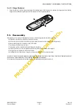
Page 9: ... 5 2 1 Lower Case Removal 1 Remove the battery from the phone 2 Remove the two grey screw caps and discard 3 Remove the four case screws and retain for re use 4 Separate the case and cover using the Separation Tool as shown 5 2 2 Antenna Removal 1 Apply pressure to the lug in the direction shown to release the antenna from the case 10631 1 10645 1 10633 1 ...

Page 10: ...er and speaker 5 2 4 Vibrate Motor Removal 1 The Vibrate motor may be lifted from the case by gently applying pressure under the body Do not lift the unit by the counterweight spindle as it may bend the spindle 5 2 5 Main PCB Removal 1 Carefully hinge the Main PCB over and lay the the pcb on a flat surface ensuring no strain is placed on the flexible connector 2 Disconnect the flexible connector a...

Page 11: ...led away from the case front 5 2 7 Display Removal 1 Open the phone 2 Remove the four grey screw caps and discard 3 Remove and retain the four screws Note that the two screws at the top of the display are smaller and blue in colour 4 Close the phone 5 Carefully prise apart the lower back case and the lower front cover creating a gap at the base of the I O connector 6 Separate the case and cover us...

Page 12: ...imilar blunt object press the lugs on the side of the Flexi PCB to release it from the upper front cover 5 2 9 Sub LCD Removal 1 Release the Sub LCD connector on the Flexi PCB 2 Release the white Sub LCD by pressing the lug 3 Lift the LCD clear ensuring the flexible connector disengages 4 Disconnect the LCD LED connector from the Flexi PCB and lift clear 5 2 10 Receiver Earpiece Removal 1 Depress ...

Page 13: ... Roll the connector end of the Flexi PCB round to enable the excess to be located in the hinge cavity Ensure earth springs are in position in the LCD holder The vibrate unit contacts are not bent The speaker cushion is placed with mesh facing the moulding All securing screws are not over tightened as this may affect the operation of the keypad The hinge pins are replaced in their correct sides On ...

Page 14: ...used for PCB testing and the 4 8 V switch setting is used for testing the complete unit 2 Interface Box IFB004 is a later version that provides 4 8 V 7 2V and 8 2 V DC outputs It also allows selection of external power via the Interface cable 3 RS 232 interface Ensures that the Unit Under Test is supplied with the correct signal levels and format Section 6 2 Lead Free PbF solder Identification and...

Page 15: ...the PCB Assembly and external test equipment It is required for RF calibration Figure 6 2 PCB Repair Jig A cable with an N Type male connector and SMA female connector will be required to make the RF connection between the Repair Jig and service equipment A replacement RF Probe for the Repair Jig is available as a spares item Caution The power cable has a large capacitor across the positive and ne...

Page 16: ...rolled light source for calibration of the camera GSM Tester This unit acts as a base station providing all the necessary GSM signalling requirements and also provides GSM signal measuring facilities Channel Box Software This is the test software for the telephone unit and should be installed onto the personal computer to be used for testing Case Separation Tool Part No JT00059 The Case Separation...

Page 17: ...ndows 95 98 or NT 5 RS232 interface cable 9 pin straight through connection 6 GSM test station 7 Panasonic Channel Box software for Microsoft Windows The Channel Box software should be installed onto the main drive of the personal computer The RF cable is connected to the GSM test station via a suitable adaptor The 12 V supply is connected to the rear socket of the Interface box 6 4 2 Using the Ch...

Page 18: ...he SELECT MODEL button on the main screen In the pop up window select GD87 or GU87 from the list box and click on the OK button 6 Click on the HANDSET POWER button and within one second switch on the handset using the key 7 Check that the handset is powered up LCD is backlit and all LEDs are on The Channel Box should also display handset IMEI number and Firmware version information in the left han...

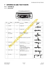
Page 19: ...ry Voltage Supply input DATA_MODE0 Data Accessory Recognition 0 5 nACC_SENSE Handsfree Data Accessory detection 6 nAUDIO ON Audio Path Control L On un mute Hi Z Off mute 7 SERIAL UP Upward serial 9600 bps SMS cable 33 8 kbps Data adaptor I F Card up to 38 4 kbps Soft Modem cable 57 6 kbps Test Command 8 SERIAL DOWN Downward serial Baud rate same as SERIAL UP 9 ACC_PWR Peripheral power supply on le...

Page 20: ...nection Status 1 VDD POWER SUPPLY IOTA D28IO 2 VDD POWER SUPPLY IOTA D28IO 3 VDD POWER SUPPLY IOTA D28IO 4 VSS COMMON GROUND GND 5 VSS COMMON GROUND GND 6 VSS COMMON GROUND GND 7 nCS CHIP SELECT SIGNAL ADDRESS DECODER nCS_LCD LCD drv chip select signal 8 RS REGISTER SELECT CALYPSO A16 DATA COMMAND reg select 9 nWR negative WRITE CALYPSO nWR 10 nRD negative READ CALYPSO nOE 11 DB8 DATA BUS 8 CALYPS...

Page 21: ...gnal NC Pin Signal PCB LCD Function Connection Status 1 VSS COMMON GROUND GND 2 VSS POWER SUPPLY IOTA D28IO 3 VSS SERIAL DATA CALYPSO DOUT 4 SCLK SERIAL CLOCK CALYPSO SCLK 5 A0 DATA SELECTION CALYPSO RS_SUB 6 nRES negative Reset signal CALYPSO nRESET 7 nCS1 negative CHIP SELECT signal CALYPSO nCS_SUB Pin Signal PCB LCD Function Connection Status 1 2 3 5 6 7 SIM CONNECTOR SIM CARD 10649 1 PIN 1 2 3...

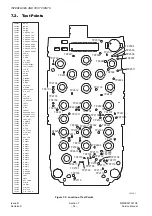
Page 22: ... TP2203 TP2301 TP2302 TP2303 TP2305 TP2306 TP2307 TP2308 TP2309 TP2311 TP2313 TP2314 TP2315 TP2316 TP2317 TP2318 TP2319 TP2320 TP2401 TP2402 TP2503 TP2504 TP2505 TP2506 TP2507 TP2508 TP2509 TP2510 TP2511 TP2601 TP2611 TP2612 TP2613 TP2614 TP2615 TP2616 TP2617 TP2618 TP2619 TP2620 TP2621 TP2622 TP2623 TP2624 TP2625 TP2626 TP2701 TP2702 TP2703 TP2704 TP2705 TP2706 TP2707 TP2708 TP2709 TP2710 BDLIP B...

Page 23: ...ED FROM THE PCB AT ANY TIME THEY MUST BE REPLACED BY NEW ITEMS ONCE REMOVED THE SHIELDS MUST NOT BE REUSED Battery calibration includes checks on voltage temperature and charging These procedures are described in Section 8 3 Adjustment data selected during calibration is stored in Flash ROM 8 2 Carrier Power Calibration 8 2 1 General Information Tx Calibration can be performed manually or automati...

Page 24: ...5 32 75 32 5 33 0 6 31 0 30 5 31 5 7 29 0 28 5 29 5 8 27 26 5 27 5 9 25 24 5 25 5 10 23 22 5 23 5 11 21 20 5 21 5 12 19 18 5 19 5 13 17 16 5 17 5 14 15 14 5 15 5 15 13 12 5 13 5 16 11 10 5 11 5 17 9 8 5 9 5 18 7 6 5 7 5 19 5 4 5 5 5 Power Level PL Output Power dBm Nominal Target Min Max 0 29 75 29 5 30 0 1 28 0 27 5 28 9 2 26 0 25 5 26 5 3 24 0 23 5 24 5 4 22 0 21 5 22 5 5 20 0 19 5 20 5 6 18 0 17...

Page 25: ...electing the Run Auto Cal button 5 Once the automatic calibration has finished select the Run Auto Verify button to verify the calibration 6 When finished select the EXIT button to save data to the handset A confirmation message will be displayed in the next box Power Level PL Output Power dBm Nominal Target Min Max 0 29 25 29 0 29 5 1 28 0 27 5 28 5 2 26 0 25 5 26 5 3 24 0 23 5 24 5 4 22 0 21 5 2...

Page 26: ...On completion of manual calibration the Verification procedure MUST be followed as detailed in Section 8 2 4 8 2 4 Manual Verification Procedure 1 If the Manual Calibration screen is not already open carry out steps 1 to 5 of Section 8 2 3 2 Select the VERIFY Button 3 Read the expected power and check against the power meter value 4 If the values are not correct adjust them by selecting the TRIM b...

Page 27: ...erature Cal failed the calibration procedure has failed Check all test equipment connections and that the correct resistor has been selected before suspecting a problem with the handset Further information may be displayed in the dialogue window 4 When the message Temperature Cal Done is displayed in the dialogue window the calibration procedure has been completed 8 3 3 Voltage and Current MDAC Ca...

Page 28: ...R FRONT COVER M201 LOWER FRONT COVER M126 LCD PANEL PROTECT SHEET M109 LCD PANEL M111 RECEIVER HOLDER M122 CAMERA HOLDER M110 LCD CUSHION M112 RECEIVER CUSHION M117 SCREW UPPER CASE M119 SCREW UPPER CASE 4mm M204 HINGE RIGHT HAND M205 HINGE LEFT HAND M103 3CF001010AAA SUB LCD PANEL M124 3CH001003AAA LCD HOLDER M128 3CW001009AAA EARTH SPRING M203 3MB001005AAA KEYSHEET M210 3DJ001001AAA ANTENNA CONT...

Page 29: ...rts 9 3 PCB Variants Network specific SIM locked PCB Assemblies are available please refer to Panasonic spares representative for details Ref No Part No Part Name Description D GD87BRD001A PCB ASSY LANGUAGE PACK A D GD87BRD001B PCB ASSY LANGUAGE PACK B D GD87BRD001C PCB ASSY LANGUAGE PACK C D GD87BRD001D PCB ASSY LANGUAGE PACK D ...

Page 30: ...CIRCUIT DIAGRAMS MMCD021001C8 Section 10 Issue B Service Manual 47 Revision 0 10 CIRCUIT DIAGRAMS Figure 10 1 Circuit Diagram RF ...

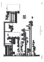
Page 31: ...CIRCUIT DIAGRAMS Issue B Section 10 MMCD021001C8 Revision 0 48 Service Manual Figure 10 2 Circuit Diagram Logic ...

Page 32: ...CIRCUIT DIAGRAMS MMCD021001C8 Section 10 Issue B Service Manual 49 Revision 0 Figure 10 3 Circuit Diagram Flexi PCB ...

Page 33: ...LAYOUT DIAGRAMS MMCD021001C8 Section 10 Issue B Service Manual 50 Revision 0 11 LAYOUT DIAGRAMS Figure 11 1 Main PCB Layout Side A ...

Page 34: ...LAYOUT DIAGRAMS Issue B Section 10 MMCD021001C8 Revision 0 51 Service Manual Figure 11 2 Main PCB Layout Side B ...

Page 35: ...LAYOUT DIAGRAMS Issue B Section 10 MMCD021001C8 Revision 0 52 Service Manual Figure 11 3 LCD PCB Layout ...

Page 36: ......

Page 37: ...MMCDE UK021002000PJ ...

Reviews: