HERCULES
MCUK001001G8
Section 7
Issue 1
Technical Guide
– 27 –
Revision 0
7 HERCULES
7.1.
Introduction
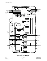
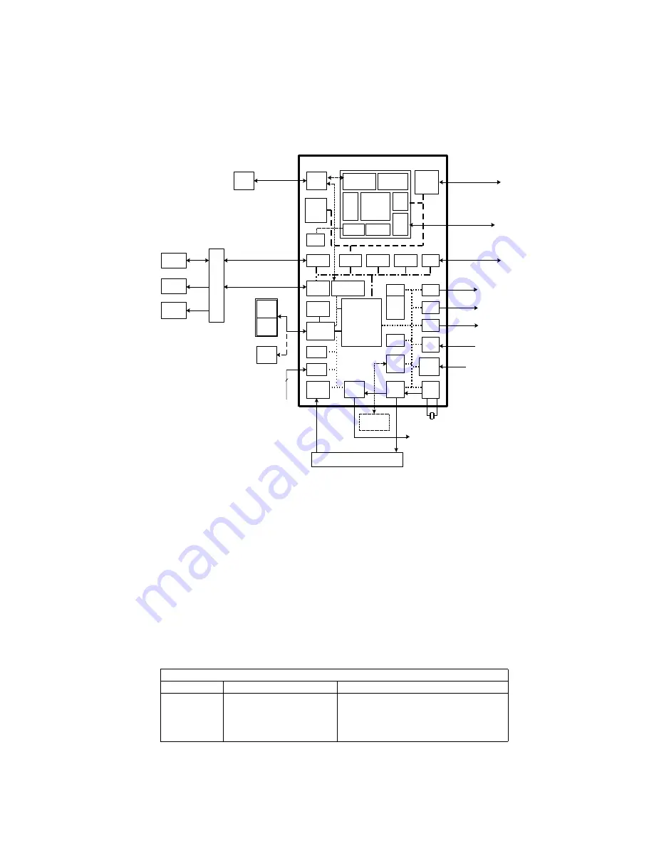
Hercules contains the DSP, CPU and GSM timing functions, and many peripheral functions. The software for the DSP is
contained in masked ROM.
Figure 7.1: HERCULES Block Diagram
7.2.
Digital Signal Processor
The Digital Signal Processor (DSP) core is compatible with a GSM chipset designed by Texas Instruments. Included in the
DSP core is an interface to the CPU by a shared memory interface.
The DSP memory is also located within HERCULES. The ROM code size is determined by the size of the software.
7.3.
CPU
The CPU is an ARM7 32-bit RISC CPU with 16-bit instruction set. The CPU is designed to access 32-bit memory and
peripherals, a further module within the HERCULES chip allows access to 8 or 16-bit memory. CPU clock speed is selectable
and is set to achieve optimum speed for memory access.
For 90 ns access FLASH and RAM, a 8.67 MHz clock gives no wait state access to both devices. Debugging access for the
CPU is provided via the JTAG interface.
Memory Access Times
Clock Speed
Memory Access Time
Additional Access time per wait state
13 MHz
67 ns
77 ns
8.67 MHz
105 ns
115 ns
6.5 MHz
144 ns
154 ns‘3
3.25 MHz
298 ns
308 ns
SPI
CPU
CORE
ROM
&
RAM
API
PLL &
CLOCKS
XIO
TEST &
EMULATION
LEAD Megamodule
TEST &
EMULATION
DMA
ARM
CORE
RIF
TPU
TDMA
TIME-
BASE
MEMORY
I/F
RTC
ARM I/O
SIM
I/F
VOICEBAND
SERIAL I/F
BASEBAND SERIAL I/F
MCU
SERIAL I/F
ULPD
IRQ
KEYPAD
BACK-
LIGHT
HERCULES-ROM2
LCD
TEST
MOBILE2
JTAG
CLOCK
GEN.
13MHz
nINT1
KEY PCB CONNECTOR
RF INTERFACE
32k X’tal
nINT2
SIM REG. &
SHIFTER
MCSI
UART
UART
IrDA
INTH
INTH
WDT
CLKM
SLICER
uWIRE
I/F
SPI
TIMER2
TIMER1
TSP
UART
Modem
PWT
PWL
TSP
PWT
PWL
LPG
JTAG
SRAM
256k*8
FLASH
1M*16
MCP
RF_EN
ACC. ASIC
SRAM
2M
FLASH
1M*16
U601
10208-1
(GD92C
only)
Summary of Contents for EB-GD93
Page 46: ...Printed in UK UK001001500PJ...


