background image

14

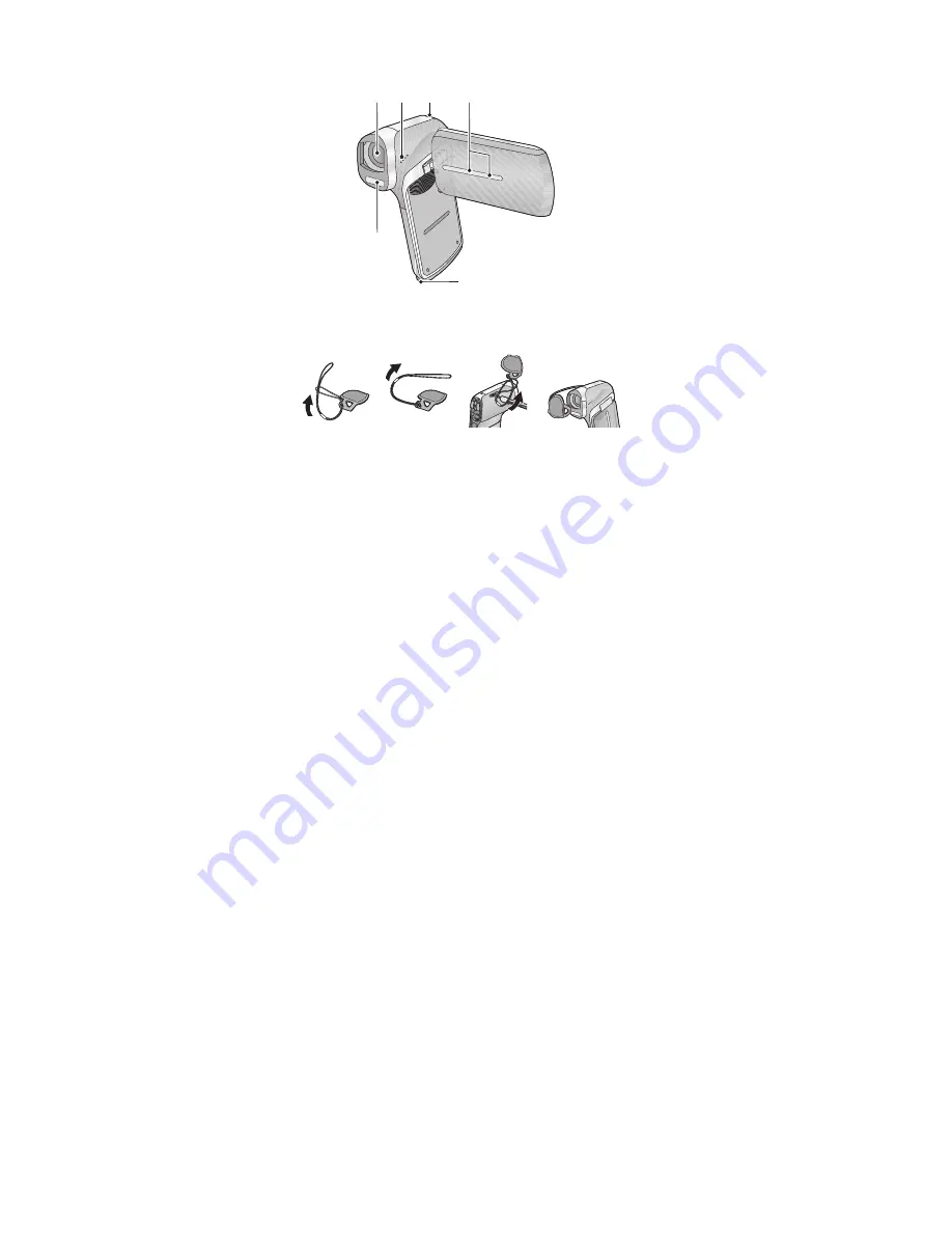
16 Lens

When not using the unit, be sure to fit the lens cap to protect the lens.

Keep the lens cap out of reach of children to prevent swallowing.

17 Speaker
18 Status indicator
19 Internal stereo microphones
20 Built-in flash

The flash reaches high temperatures and may cause burns if touched.
Please do not touch the flash.

21 Tripod receptacle

If you attach a tripod which has a 5.5 mm (0.22

S

) screw or larger, it

may damage this unit.

19

17

16

18

20

21


Summary of Contents for HX-DC2PP

Page 1: ...and distribution is a violation of law ORDER NO VM1202007CE B27 Dual Camera Model No HX DC2PP HX DC2PU HX DC2EB HX DC2EC HX DC2EE HX DC2EF HX DC2EG HX DC2GA HX DC2GC HX DC2GD HX DC2GK HX DC2GN HX DC2G...

Page 2: ...PbF 7 3 3 Important Notice 1 Other than U S A and Canadian Market 7 3 4 How to Define the Model Suffix NTSC or PAL model 8 3 5 Formatting 9 4 Specifications 10 5 Location of Controls and Components 1...

Page 3: ...g exposed to shock hazards 1 2 Leakage Current Cold Check 1 Unplug the AC cord and connect a jumper between the two prongs on the plug 2 Measure the resistance value with an ohmmeter between the jumpe...

Page 4: ...ing Procedure 1 Refer to the disassemble procedure and Remove the necessary parts unit 2 Put the insulation tube onto the lead part of Resistor ERG5SJ102 1k 5W an equivalent type of resistor may be us...

Page 5: ...y a grounded tip soldering iron to solder or unsolder ES devices 4 Use only an antistatic solder removal device Some solder removal devices not classified as antistatic ESD protected can generate elec...

Page 6: ...TE This Lithium battery is a critical component It must never be subjected to excessive heat or discharge It must therefore only be fitted in requirement designed specifically for its use Replacement...

Page 7: ...sing the lead free solder To put lead free solder it should be well molten and mixed with the original lead free solder Remove the remaining lead free solder on the P C B cleanly for soldering of the...

Page 8: ...ods To define the model suffix to be serviced refer to the rating label and caution label which are putted on the Unit NOTE After replacing the MAIN P C B or IC121 be sure to achieve update the Firmwa...

Page 9: ...9 3 5 Formatting...

Page 10: ...10 4 Specifications...

Page 11: ...11...

Page 12: ...12...

Page 13: ...ots on the LCD monitor screen However this is not a malfunction and does not affect the recorded picture 1 2 3 4 5 Hand strap fixture 6 Zoom range button 7 Photoshot button 8 SET button SET Use the SE...

Page 14: ...to prevent swallowing 17 Speaker 18 Status indicator 19 Internal stereo microphones 20 Built in flash The flash reaches high temperatures and may cause burns if touched Please do not touch the flash 2...

Page 15: ...e and adjustment 1 The firmware together with version up procedure are available at software download on the Support Information from NWBG VDBG AVC web site in TSN system 2 The adjustment instruction...

Page 16: ...16 7 Disassembly and Assembly Instructions 7 1 Disassembly Flow Chart This is a disassembling chart When assembling perform this chart conversely 7 2 PCB Location...

Page 17: ...901 Connector CN951 Flex Lens Unit 2 Lens Holders 9 Main P C B Fig D12 2 Screws J 2 Solders 1 Locking tab Fig D13 CN103 Connector CN301 Flex Main P C B 10 Speaker Fig D14 1 Screw K Speaker Earth Speak...

Page 18: ...18 7 3 1 Removal of the Side Case L Battery Cover and USB Cover Fig D1 Fig D2...

Page 19: ...19 Fig D3 Fig D4 7 3 2 Removal of the Battery Frame Fig D5...

Page 20: ...20 7 3 3 Removal of the Battery Terminal P C B Fig D6 7 3 4 Removal of the Heat Sink Left Fig D7...

Page 21: ...21 7 3 5 Removal of the Flash P C B Fig D8 7 3 6 Removal of the Battery Terminal Holder Fig D9 7 3 7 Removal of the Front Case Unit Fig D10...

Page 22: ...22 7 3 8 Removal of the Lens Unit Fig D11 7 3 9 Removal of the Main P C B Fig D12 Fig D13...

Page 23: ...23 7 3 10 Removal of the Speaker Fig D14 7 3 11 Removal of the Operation Unit Fig D15 7 3 12 Removal of the Side Cover R and Grip Cover Fig D16...

Page 24: ...24 Fig D17 7 3 13 Removal of the LCD Unit Fig D18 7 3 14 Removal of the LCD Hinge Unit Fig D19...

Page 25: ...25 Fig D20 7 3 15 Removal of the LCD Panel Fig D21 Fig D22 7 3 16 Removal of the Monitor P C B Fig D23...

Page 26: ...26 Fig D24 7 3 17 Removal of the Mic Fig D25...

Page 27: ...with PC Connection method of the main unit and an exclusive adjustment jig as follows 8 1 1 Adjustment Procedure Connect the main unit to PC with USB The adjustment instruction is available at Softwar...

Page 28: ...stment item as follows The adjustment instruction is available at Software download on the Support Information from NWBG VDBG AVC web site in TSN System The firmware together with version up procedure...

Page 29: ...BATTERY HINGE MAGNET IC303 HALL SENSOR PANEL OPEN CLOSE DETECT PANEL_OPEN IC501 SWITCHING CONTROL PWA BLOCK POWER MANAGEMENT RTC CEC HPD SP SP DDC_ SDA SCL CN801 CN110 USB HOST CONTROL HDMI AUDIO CODE...

Page 30: ...S_DATA2 TMDS_DATA1 TMDS_DATA0 SDCLK SDCMD SDWP SDDET SWITCH UNIT BSRST EXCLKS XOUT XIN L R _OUT LENS_12M PON RED GREEN _LED SLVSD 0 3 N SLVSD 0 3 P SLVSC N P ADCK RESET_N TGVD CMOS_SDA CMOS_SCL MIC_ L...

Page 31: ...IMAGE SENSOR LENS BLOCK DIAGRAM HX DC2 LENS BLOCK DIAGRAM LENS_TEMP LENS_SOUT ZOOM MOTOR FOCUS MOTOR IRIS ZOOM_A ND ZOOM_B ZOOM_B ZOOM_A FOCUS_A FOCUS_B FOCUS_B FOCUS_A ND VDD3 VDD3 OUT1A OUT3A OUT1B...

Page 32: ...UT5 CMOS1 8 IC502 IC505 REG VDD1 5 PVIN4 L5031 STEP DOWN CIRCUIT SW3 VDD1 1 L5041 STEP DOWN CIRCUIT SW4 VAA2 8 SYS 1 CE 3 CE 1 VOUT 3 VOUT VIN 4 VIN 4 IC501 SWITCHING CONTROL TO DMA TO DMA TO DMA XIN...

Page 33: ...ND 29 ADCK 30 GND 31 SDA 32 SCL 33 RESET_N 34 GND 35 GND 36 GND 37 TGVD 38 GND 39 GND 40 GND 41 AGND 42 AGND 43 VAAPIX 44 VAAPIX JW185 1 SP JW186 1 SP CN171 1 VCOM 2 CS 3 SDA 4 SCL 5 HSYNC 6 VSYNC 7 D...

Page 34: ...Model No HX DC2 Schematic Diagram Note...

Page 35: ...Model No HX DC2 Parts List Note...

Page 36: ...Model No HX DC2 Main CAA Schematic Diagram Main P C B...

Page 37: ...Model No HX DC2 Main DMA Schematic Diagram Main P C B...

Page 38: ...Model No HX DC2 Main PWA Schematic Diagram Main P C B...

Page 39: ...Model No HX DC2 Flash Schematic Diagram Flash P C B...

Page 40: ...Model No HX DC2 Monitor Schematic Diagram Monitor P C B...

Page 41: ...Model No HX DC2 Main P C B Component Side...

Page 42: ...Model No HX DC2 Main P C B Foil Side...

Page 43: ...Model No HX DC2 Flash P C B Component Side...

Page 44: ...Model No HX DC2 Flash P C B Foil Side...

Page 45: ...Model No HX DC2 Monitor P C B Component Side...

Page 46: ...Model No HX DC2 Monitor P C B Foil Side...

Page 47: ...3V 4 7U 1 C1047 VU3033846508 C CAPACITOR 1 C1048 VU3033846508 C CAPACITOR 1 C1071 F1G0J1050007 C CAPACITOR CH 6 3V 1U 1 C1072 F1G1A1040006 C CAPACITOR CH 10V 0 1U 1 C1073 F1G1A1040006 C CAPACITOR CH 1...

Page 48: ...C5011 F1G0J1050007 C CAPACITOR CH 6 3V 1U 1 C5021 VU3033846508 C CAPACITOR 1 C5022 F1J0J2260004 CAPACITOR 1 C5031 VU3033846508 C CAPACITOR 1 C5032 F1J0J2260004 CAPACITOR 1 C5033 F1J0J2260004 CAPACITOR...

Page 49: ...1 B0JCDD000019 DIODE 1 E S D F5001 K5H252Z00003 FUSE 1 F5002 K5H102Z00006 FUSE 1 F5004 K5H202Z00005 FUSE 1 F5009 K5H502Z00003 FUSE 1 IC101 C1AB00003893 IC 1 E S D IC103 C3ABTY000074 IC 1 E S D IC104 C...

Page 50: ...RESISTOR 1 R1031 VU3012864400 RESISTOR 1 R1032 D0GA103JA042 RESISTOR 1 R1034 D0GA103JA042 RESISTOR 1 R1037 D0GA101JA042 RESISTOR 1 R1038 D0GA103JA042 RESISTOR 1 R1039 D0GA102JA042 RESISTOR 1 R1045 D0...

Page 51: ...A042 RESISTOR 1 R5434 D0GA563ZA029 RESISTOR 1 R5435 D0GA243ZA029 RESISTOR 1 R5436 D0GA821ZA029 RESISTOR 1 R6301 D0GA102JA042 RESISTOR 1 R8001 D0GA103JA042 RESISTOR 1 R8002 D0GA273JA042 RESISTOR 1 R800...

Page 52: ...1 RB171 VU9450280697 RESISTOR NETWORKS 1 RB172 VU9450280697 RESISTOR NETWORKS 1 RB541 VU9450280703 RESISTOR NETWORKS 1 S3001 K0F111A00547 SWITCH 1 T5401 VU6451011008 TRANSFORMER 1 TH301 VU3080547700 T...

Page 53: ...Model No HX DC2 Frame and Casing Section 1...

Page 54: ...Model No HX DC2 Frame and Casing Section 2...

Page 55: ...Model No HX DC2 Packing Parts and Accessories Section...

Page 56: ...LABEL 1 GK 20 VU6451048813 SPEAKER 1 21 VU6451052506 OPERATION UNIT 1 H 21 VU6451052513 OPERATION UNIT 1 W 22 VU6361495868 MIC EARTH 1 23 VU6361518161 SHEET 1 24 VU6361518161 SHEET 1 25 VU6451043306 L...

Page 57: ...PU H GT H EG H EF H EC H EB H GA H E E H GN H 103 VPG3F15WKIT PACKING CASE 1 PU W GT W EG W EC W EB W GA W 103 VPG3F15DHKIT PACKING CASE 1 GD H GC H 103 VPG3F15DWKIT PACKING CASE 1 GD W GC W 103 VPG3...

Page 58: ...6909 SCREW 1 B23 VU4111990908 SCREW 1 B24 VU4111990908 SCREW 1 B25 VU4111786204 SCREW 1 B26 VU4111786204 SCREW 1 B27 VU4111840005 SCREW 1 B28 VU4111840005 SCREW 1 B29 VU3120607906 SCREW 1 B30 VU312060...

Reviews: