Pig ta il leading
(1) Pass the pig tail th ro u g h the pig ta il clamp.
(See Fig. 12-9-1.)
(2) Locate the side 0 to the outer side and side 1 to
the inner side, provide a clearance o f 1mm
between them, and place them parallel to each
other.
(Avoid tw isting or closing.)
(3) Fig. 12-9-2
[When the carriage is on the outer-m ost track]
(a) When the head carriage is on the o u te r
most track, lead the side 0 and side 1 along
line A on the pig tail clamp.
(b) Ensure th a t the pig ta il does not come in
contact w ith the inner w a ll o f the base.
(Contacting o f the pig tail is allow able if
the side 0 and side 1 are n ot overlapped
each other vertically.)
(4) Fig. 12-9-2
[When the carriage is on the inner-most track]
(a) When the head carriage is on the in n e r
most track, lead the side 0 and side 1 along
line B on the pig tail clamp.
(5) Provide a clearance o f about 1mm between the
side 0 and side 1.
(6) Ensure th a t th e re is n o t excessive load or
protrusion at the o u tle t fo r the pig tail in the
head carriage.
(7) Fasten the pig tail clamp w ith screw.
(8) Do not pull the pig ta il by a force more than
500g a fte r it has been clamped.
(9) Pull the pig tail lig h tly to ensure th a t it does
n ot move.
Summary of Contents for JU-475-4
Page 1: ...ORDER NO MSD891122000 Service Manual Flexible Disk Storage Drive JU 475 4 Panasonic ...
Page 6: ...6 2 Troubleshooting Flowchart Table6 1 Troubleshooting Flowchart 4 ...
Page 14: ...10 TEST POINTS Printed Circuit Board Top View GND Vout Vout GND TRK0 TP 8 kJ 1 2 ...
Page 30: ...17 CIRCUIT BOARD JU 475 4AGG Component Side Top 28 TP5 L 6 ...
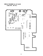
Page 31: ...CIRCUIT BOARD JU 475 4AGG Solder Side Bottom 29 ...
Page 34: ...Matsushita Communication industrial Co Ltd Memory Systems Division ...


