|
62
|
KX-F680BX/KX-F2681BX
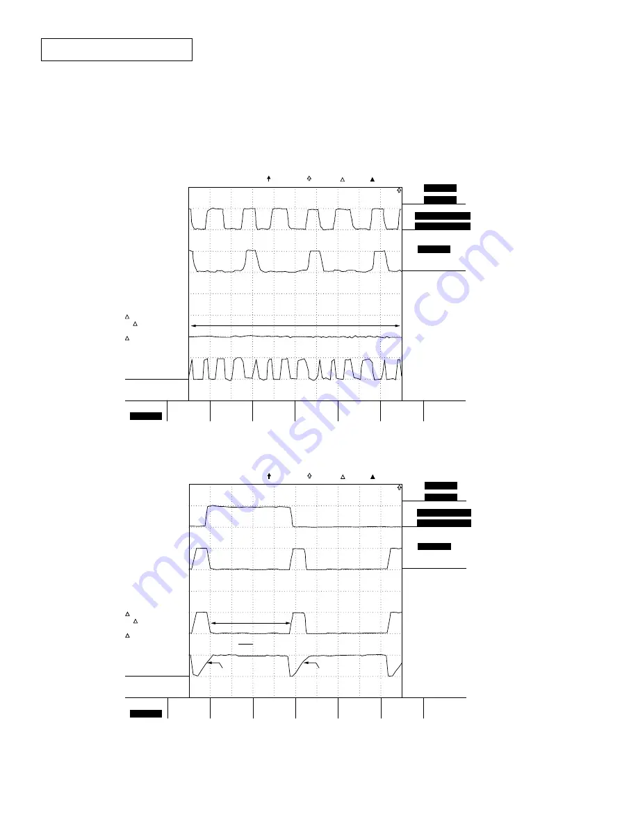
The graphs below show you the wave form that is observed when unit (board) doesn't work. (A3 is intentionally opened at
pin 135 of ASIC in this board.)
Please check that active (low level) term of ROMCE is longer than good wave form, **ROMCE is active (low level) except-
ing RESET is active.** and RESET is frequently coming on every 4 msec.
In the case of this wave form ASIC (IC1), ROM (IC2) or on the way of bus line route is possibly defect. If soldering, con-
ductance is no problem, we need to replace these ICs.
CH1 5V/div
CH2 5V/div
CH3 5V/div
CH4 5V/div
W1 500ns/div
Length 100
W2 5
µ
s/div
Length 1k
Sampling
Normal
20Msps
Marker 1
T 9.65
µ
s
V 4.7 V
Marker 2
T 7.50
µ
s
V 4.9 V
T -2.15
µ
s
1/ T
465.1k Hz
V 0.2 V
W1
500µs
W2
5µs
Position
W1
6.20µs
W2
25.00µs
Time
Time Base
Roll
Off
Time Base
External
Internal
Internal
-39.9V
6.20
µ
s
11.20
µ
s
Time/div
10.0V
H1 W1
A0
D0
ROMCS
RD
NG
Trigger CH1/2 MEM1 MEM2
Too long
CH1 5V/div
CH2 5V/div
CH3 5V/div
CH4 5V/div
W1 1ms/div
Length 100
W2 10ms/div
Length 1k
Sampling
Normal
10ksps
Marker 1
T 576.5ms
V 4.8 V
Marker 2
T 15.0ms
V 0.2 V
T -561.5ms
1/ T
1.781 Hz
V -4.6 V
W1
1ms
W2
10ms
Position
W1
575.0ms
W2
50.2ms
Time
Time Base
Roll
Off
Time Base
External
Internal
Internal
-40.0V
575.0ms
585.0ms
Time/div
10.0V
H1 W1
A0
D0
ROMCS
RST
RESET
RESET
NG
Trigger CH1/2 MEM1 MEM2
Too long
Summary of Contents for KX-F2681BX
Page 1: ......
Page 11: ......
Page 106: ......
Page 107: ......
Page 108: ......
Page 109: ......
Page 110: ......
Page 111: ......
Page 112: ......
Page 113: ......
Page 114: ......
Page 115: ......
Page 116: ......
Page 117: ......
Page 118: ......
Page 119: ......
Page 120: ......
Page 121: ......
Page 122: ......
Page 123: ......
Page 124: ......
Page 125: ......
Page 126: ......
Page 127: ......
Page 128: ......
Page 129: ......
Page 130: ... 165 KX F680BX KX F2681BX EC1 EC2 EC3 EC4 EC5 EC6 EC7 EC9 EC10 EC11 EC12 EC13 EC8 TOOLS ...
Page 131: ......
Page 133: ......
Page 134: ......
Page 135: ......
Page 136: ......


