background image

22

KX-PRL260/KX-PRL262/KX-PRD260/KX-PRD262/KX-PRLA20

4.8.

Circuit Operation (Handset)

4.8.1.

Outline

Handset consists of the following ICs as shown in 

Block Diagram (Handset)

 (P.20).

• DECT BBIC (

B

ase 

B

and IC): IC1

- All data signals (forming/analyzing ACK or CMD signal)
- All interfaces (ex: Key, Detector Circuit, Charge, EEPROM, LCD)

• EEPROM: IC3

- Setting data is stored. (e.g. ID, user setting)

4.8.2.

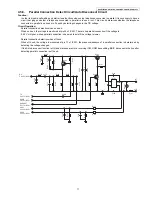
Power Supply Circuit/Reset Circuit

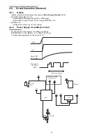
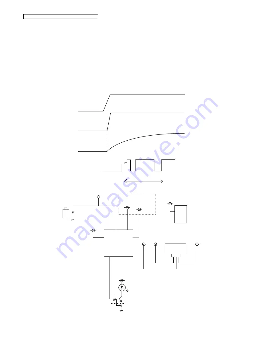
Circuit Operation:

When powering on the Handset, the voltage is as follows;
BATTERY(2.2 V ~ 2.6 V: BATT+) 

 F1 

 BBC1 (IC1) 10 pin

The Reset signal generates IC1 (54 pin) and 1.8 V.

Start monitor

(IC1 50 pin)

1.8 V

VBAT

Reset (*RST) 
(IC1_71 pin)

BBIC chip initialize

(STM)

GND

BATTERY
2CELL

BBIC

3.0V

3.0V

Charge Pump Output
For all peripherals

3.0V

3.0V

EEPROM

GND

KEY LED

4.0V

VBAT

1.8V

3.0V

3.0V

LCD

4.0V

4.0V

1.8V

Summary of Contents for KX-PRD260B

Page 1: ...iPhone PRD series Link to Cell Docking Station for Smartphone B Black Version W White Version for U S A Base Unit KX PRD260 Base Unit KX PRL260 Charger Unit Handset KX PRLA20 KX PRLA20 is also an optional accessory which contains a handset and a charger KX PRLA20 1 PRLA20 1 Up to 6 KX PRD262 1 PRD260 1 PRLA20 1 Up to 6 KX PRD260 1 PRD260 1 PRLA20 Up to 6 KX PRL262 1 PRL260 1 PRLA20 1 Up to 6 KX PR...

Page 2: ...ematic Diagrams Circuit Board Diagrams Exploded Views and Replacement Parts List It is essential that these critical parts should be replaced with manufacturer s specified parts to prevent shock fire or other hazards Do not modify the original design without permission of manufacturer IMPORTANT INFORMATION ABOUT LEAD FREE PbF SOLDERING If lead free solder was used in the manufacture of this produc...

Page 3: ...ering a Handset to the Base Unit 42 10 1 8 Deregistering a Handset 42 10 1 9 Check Handset Transmission 43 10 1 10 Check Handset Reception 43 10 1 11 Check Caller ID 43 10 1 12 Check BT Communication 44 11 Disassembly and Assembly Instructions 46 11 1 Disassembly Instructions 46 11 1 1 Base Unit 46 11 1 2 Handset 48 11 1 3 Charger Unit 49 11 2 How to Replace the Handset LCD 50 12 Measurements and ...

Page 4: ...l Parts Base Unit 80 16 2 Cabinet and Electrical Parts Handset 81 16 3 Cabinet and Electrical Parts Charger Unit 82 16 4 Accessories and Packing Materials 83 16 4 1 Tools KX PRL260 262 KX PRD260 262 83 16 4 2 Tools KX PRLA20 84 16 5 Replacement Parts List 85 16 5 1 Base Unit 85 16 5 2 Handset 88 16 5 3 Charger Unit 89 16 5 4 Accessories and Packing Materials 89 16 5 5 Screws 89 16 5 6 Fixtures and...

Page 5: ... product you have purchased Please call 1 800 8 BATTERY 1 800 822 8837 for information on how to recycle this battery 2 2 About Lead Free Solder PbF Pb free Note In the information below Pb the symbol for lead in the periodic table of elements will refer to standard solder or solder that contains lead We will use PbF solder when discussing the lead free solder used in our manufacturing process whi...

Page 6: ...n Zn Bi Please check the manufacturer s specific instructions for the melting points of their products and any precautions for using their product with other materials The following lead free PbF solder wire sizes are recommended for service of this product 0 3 mm 0 6 mm and 1 0 mm 2 3 Discarding of P C Board When discarding P C Board delete all personal information such as telephone directory and...

Page 7: ...Weight AC Adaptor PNLV238 KZ 120 V AC 60 Hz Super Heterodyne PLL synthesizer Quadrature Discriminator 10 368 MHz 100 Hz Frequency Modulation 40 bit 0 1 B Tone DTMF Pulse Up to 48 digits Up to 24 digits Phonebook Standby Approx 1 1 W Maximum Approx 13 5 W 0 C 40 C 32 F 104 F 20 80 relative air humidity dry Approx 160 mm x 100 mm x 115 mm for KX PRL262 PRD262 Approx 330 g for KX PRL262 PRD262 Base U...

Page 8: ... is performed Handset doesn t make up duplex in no free RF channels because of interference 1 Dummy Bearer Base unit sends Dummy data to the all stand by state handsets Handsets receive that data for synchronization and monitoring request from the base unit Base unit doesn t send Dummy bearer in no free RF channels because of interference 1 Note 1 It is a feature under FCC 15 regulation and for in...

Page 9: ...t to digital data RXDATA BBIC IC1 converts RXDATA into a voice signal and outputs it to speaker Transmission Handset A voice signal from microphone is encoded to digital data and converted into a 1 9 GHz modulated radio signal by BBIC IC1 The RF signal after which is amplified in BBIC is fed to an antenna Base unit As for a base unit RF RF signal is received in two antennas BBIC IC501 compares RF ...

Page 10: ...8MHz TR_RLY TIP RING TEL_JACK VRF VPA RF_Block IC501 BBIC DC5 5V GND DC_JACK CHARGE 3 4 2 1 D101 CHARGE DETECT Q701 Q141 Q161 REGULATOR IC302 Power Down DET Power supply at AC failure KEY PAD LED VBAT PDN_DET CHARGE_DET IC611 IC502 IC601 IC721 BT Module Q301 1 8V 5 0V 3 0V 5 0V 5 0V AVD VDD QSPI CIDINp CIDINn P3_6 MICh LSRp RF_VDD VDD_PA ANT2 IC722 BT_1 8V IC411 IC402 IC401 ...

Page 11: ...RD260 KX PRD262 KX PRLA20 4 3 Tel Interface Circuit TX AMP SIDE TONE RX AMP CONTROL CIRCUIT CALLER ID DETECT BELL DETECT P101 R142 3 4 2 1 C101 Q141 C102 SA101 TIP RING R141 REGULATOR C104 R102 C106 R104 C103 R101 C105 R103 D101 ...

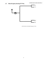
Page 12: ...PRLA20 4 4 Block Diagram Base Unit_RF Part 10 368 MHz IC501 RF block TXDATA ANT2 RF_TXp RF_TXn RF_RXp RF_RXn Control Logic RXDATA Mixer Demodulator PLL 3856 3843MHz 3859 3845MHz Modulator KX PRL260 262 KX PRD260 262 BLOCK DIAGRAM Base Unit_RF Part ...

Page 13: ...nd a Flash Memory which stored the vocabulary Caller ID demodulation The BBIC implements monitor and demodulate the FSK DTMF signals that provide CID information from the Central Office Digital Switching The voice signal from telephone line is transmitted to the handset or the voice signal from the handset is transmitted to the Telephone line etc They are determined by the signal path route operat...

Page 14: ... analog part is insulated from VBAT by Doubler of BBIC Circuit Operation 5 5V 5 5V 3 0V 3 0V 1 8V 3 0V_CP IC501 IC302 IC611 BBIC AC Adaptor 3 0V REGULATOR EEPROM VDD2 VDD1 VDD4 3 0V_CP2 IC601 TAM FLASH D AMP VDD5 VDD3 RF Part LEDs Q301 Bluetooth unit IC721 QSPI FLASH IC502 1 8V IC722 IC411 IC401 5 0V REGULATOR Startmonitor IC501 57pin 1 8 V VBAT Reset RSTN IC501_77pin BBIC chip initialize CKM STM ...

Page 15: ...5 KX PRL260 KX PRL262 KX PRD260 KX PRD262 KX PRLA20 4 5 6 1 Charge Circuit The voltage from the AC adaptor is supplied to the charge circuits R372 D362 R371 CHARGE R373 C351 F301 DCP CHARGE 5 5V DCM K A ...

Page 16: ...en Q141 is connected as to cut the DC loop current and to cut the voice signal The unit is consequently in an on hook condition Pulse Dial Circuit Pin 19 of BBIC turns Q141 ON OFF to make the pulse dialing Side Tone Circuit Basically this circuit prevents the TX signal from feeding back to RX signal As for this unit TX signal feed back from Q161 is canceled by the canceller circuit of BBIC OFF Hoo...

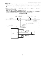
Page 17: ...ection if the voltage is 0 54 V or higher while a parallel connection is deemed to exist if the voltage is lower Parallel connection detection when off hook When off hook the voltage is monitored at pin 17 of IC501 the presence absence of a parallel connection is determined by detecting the voltage changes If the Auto disconnect function is ON and statuses are Hold receiving ICM OGM transmitting B...

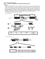
Page 18: ...is modulated in an FSK Frequency Shift Keying format Data 1 is a 1200 Hz sine wave and data 0 is a 2200 Hz sine wave There are two types of the message format which can be received i e the single message format and plural message format The plural message format allows to transmit the name and data code information in addition to the time and telephone number data Also the telephone exchange servi...

Page 19: ...ss the following route Telephone Line P101 C105 C104 R103 R102 IC501 23 21 If the unit deems that a telephone connected in parallel is in use ACK is not returned even if CAS is received and the information for the second and subsequent callers is not displayed on the portable handset display CAS CAS CPE Alerting Signal Dual Tone of 2130 Hz 2750 Hz 15 dBm 900 ohm load 80 5 ms MARK DATA 0 500 ms 58 ...

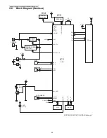
Page 20: ...T CHG_CTL BATTERY_ON CHG_DET WP CLK DATA STB_A F KIN_1 4 CHARGE MIC Receiver SP PHONE SP LCD KEYS RF part ANT1 X1 10 368 MHz EEPROM 3V BATTERY LED LCD RSTN VBAT VBAT 4V RXn RXp TXp TXn KX PRLA20 BLOCK DIAGRAM Handset KEY_LED Q6 LED KEY 4V CHARGE CONTROL POWER SUPPLY CONTROL IC4 FLASH MEMORY QSPI_100 4 QSPI_CS LSRn STM NR_LED QSPI_SCK1 ...

Page 21: ...21 KX PRL260 KX PRL262 KX PRD260 KX PRD262 KX PRLA20 4 7 Block Diagram Handset_RF Part KX PRLA20 BLOCK DIAGRAM Handset_RF Part RXp RXn ANT TXp TXn ...

Page 22: ...e EEPROM LCD EEPROM IC3 Setting data is stored e g ID user setting 4 8 2 Power Supply Circuit Reset Circuit Circuit Operation When powering on the Handset the voltage is as follows BATTERY 2 2 V 2 6 V BATT F1 BBC1 IC1 10 pin The Reset signal generates IC1 54 pin and 1 8 V Start monitor IC1 50 pin 1 8 V VBAT Reset RST IC1_71 pin BBIC chip initialize STM GND BATTERY 2CELL BBIC 3 0V 3 0V Charge Pump ...

Page 23: ...tected by BBIC which check the voltage from battery The detected voltage is as follows Battery Low Battery voltage V Batt 2 25 V 50 mV The BBIC detects this level and starts flashing Power Down Battery voltage V Batt 2 0 V 50 mV The BBIC detects this level and power down 4 8 5 Speakerphone The hands free loudspeaker at SP and SP is used to generate the ring alarm 4 9 Circuit Operation Charger Unit...

Page 24: ...e Operating Instructions Instruction book on TSN Server 6 Installation Instructions Refer to the Operating Instructions Note You can download and refer to the Operating Instructions Instruction book on TSN Server 7 Operating Instructions Refer to the Operating Instructions Note You can download and refer to the Operating Instructions Instruction book on TSN Server ...

Page 25: ...ddress 1 4 Select Write EEP using then press SELECT 3 Enter 7 2 6 2 7 6 6 4 Note 7262 7664 PANA SONI see letters printed on dial keys or Select Set tel line using then press SELECT or 2 Select Settings using then press SELECT 1 Press MENU H S key operation Important Make sure the address on LCD is correct when entering new data Otherwise you may ruin the unit This pictured model is KX PRL260 OFF D...

Page 26: ...mber hex Input Keys Desired Number hex Input Keys 0 0 A Flash 0 1 1 B Flash 1 C Flash 2 D Flash 3 E Flash 4 9 9 F Flash 5 OFF 3 Select off Select off SELECT SELECT or 2 MENU 1 5 7 1 Set tel line isn t displayed in Cell line only mode To return to normal mode execute the following procedure Note To enter Set dial mode press SELECT SELECT at Set tel line It is necessary to turn on the power of base ...

Page 27: ...t H S LCD OFF 8 Press to return to standby mode After that remove and reinsert the batteries Press the Power button for about 1 second if the power is not turned on 7 Press OK a long confirmation beep will be heard 6 Enter 㸨 㸨 New Data 1 5 Enter ە ە ە ە Address 1 or 4 Select Write EEP using then press SELECT 3 Enter 7 2 6 2 7 6 6 4 Note 7262 7664 PANA SONI see letters printed on dial keys 2 Select...

Page 28: ...D ONLY mode to confirm the contents Careless rewriting may cause serious damage to the handset Items Address Default Data New Data Possible Adjusted Value MAX hex Possible Adjusted Value MIN hex Remarks Frequency 00 07 00 08 00 01 2 ID 00 02 00 06 Given value Desired Number hex Input Keys Desired Number hex Input Keys 0 0 A Flash 0 1 1 B Flash 1 C Flash 2 D Flash 3 E Flash 4 9 9 F Flash 5 ...

Page 29: ... KX PRLA20 9 Service Mode 9 1 How to Clear User Setting Handset Only Handset Press simultaneously until a beep sound is heard Then single handset is initialized The contents of user setting are reset to factory default Usage time is not cleared ...

Page 30: ...om can not reappear with TEL simulator in the service center In this case try to change the Auto disconnect activation time and Vox level How to change the Auto Disconnect activation time and VOX level P 33 item A and B Power ON Base Unit OK FLOW CHART Check Power OK Playback Pre Message Check Playback Record OK Check Record Range Check the RF part Handset Voice Transmission Check Handset Transmis...

Page 31: ... Adaptor inserted into AC outlet 1 Is output voltage of AC adaptor 5 5 V YES Check AC Adaptor Check VDD1 1 8 V Test point VDD1 OK Check Power Supply Circuit NO NO NO NO RSTN Reset High YES Check Reset Circuit Check Xtal CLK 10 368 MHz YES Check X501 Check BBIC Check Power Supply Circuit Reset Circuit Check X1 C52 C53 Is the voltage of TP VBAT 2 3 V more Check the battery and around BATT and BATT a...

Page 32: ...ct Circuit Auto Disconnect Circuit P 17 Note Flash Memory is IC601 BBIC is IC501 Check Bell signal OK Check Telephone Line Interface Bell Does the unit catch line YES Check Telephone Line Interface OFF HOOK Check Line In Pin 25 of BBIC Check ICM Recording in Signal Route NO OK Check Auto Disconnect Circuit OK Check Parallel Connection Detection Circuit OK Check BBIC and Flash Memory NO NO ...

Page 33: ...low 1 Press MENU key at standby Mode and key Note The set must power on and be linked 2 Press 9 0 0 0 3 Press 7 3 1 4 Then enter the below last digit 5 Back to standby mode automatically after step 4 You can hear beep sound which is a confirmation tone Service ready 7 3 1 Service ready LCD H S last digit 0 Auto disconnect CPC enable 㨇default㨉 1 1 Auto disconnect CPC disable 2 1 2 Auto disconnect e...

Page 34: ...ensitivity of VOX level Therefore the recording of TAM is not turned off during detection 1 2 are same as A 3 Press 5 1 1 4 Then enter the below last digit 5 Back to standby mode automatically after step 4 You can hear beep sound which is a confirmation tone Service ready 5 1 1 last digit 0 default setting normal 1 6dB up CLEAR ...

Page 35: ...e Circuit P 23 Check VDD1 1 8 V Test point VDD1 OK Check Power Supply Circuit Check output of BBIC Pin 73 74 OK Check BBIC and Flash Memory Check Speaker and its surroundings NO NO Check VDD3 5 0 V Test Point VDD3 OK Check IC411 NO Check Charge Circuit of Base Unit Check Handset Plug in the AC Power source Charge Handset on Base Unit Is the voltage of two charge contacts about 3 V or more OK NO Ch...

Page 36: ...until the frequency counter becomes10 368 MHZ 55 HZ Check Charge Circuit of Charger Unit Check Handset Plug in the AC Power source Charge Handset on Charger Unit Is the voltage of two charge contacts about 5 5 V or more OK NO Check Charge Contacts at Charger Unit from mechanical point of view YES Check around Power Supply Circuit Does Base Unit connect to the properly working Handset Check around ...

Page 37: ...heck the TP_CKM IC1 49pin To adjust frequency send command SFR until the frequency counter becomes10 368 MHz 55 HZ Check around Power Supply Circuit Reset Circuit Does Handset link with Base Unit Properly working unit Check around X1 and RF module and adjust clock frequency NO NO NO NO Is the voltage of TP VBAT about 2 2 2 8 V Is the voltage of 1 8 V about 1 8 V YES YES YES Does the RF clock CLK o...

Page 38: ...ar BU 2 2 a Re register regular HS Normal mode to base unit to be checked If this operation fails in some ways the base unit is defective b Re register handset to be checked to regular BU Normal mode If this operation fails in some ways the handset is defective Base unit is defective Handset is defective START Registration of Regular HS to base unit Registration of handset to Regular BU other chec...

Page 39: ...t P 40 Please refer to the each item Note 1 Refer to Check Link P 36 Start Link confirmation Normal 1 Control signal confirmation X tal Frequency confirmation TX confirmation Range confirmation Normal TEST RANGE Check Check BBIC interface parts RF Block BBIC on BU HS P C B Adjust X tal Frequency 1 Check TX Block GOOD 5 2 3 4 OK OK OK NG NG NG NG NG OK OK ...

Page 40: ...al Frequency 10 368 MHz 100 Hz Check X tal Frequency 10 368 MHz 100 Hz 3 TX confirmation HS Mode HS_Burst Mode 1 BS Mode BS_Burst Mode 1 1 Remove wire antenna 2 and connect spectrum analyzer to TP 2 2 Confirm TX power whether spec is satisfied Power 13 5 dBm 1 Connect spectrum analyzer to TP 3 2 Confirm TX power whether satisfied spec Power 16 0 dBm 4 Range Confirmation Normal HS BU Mode Normal Mo...

Page 41: ...3 At distance of about 20 m between HS and BU Link OK TX Power of the HS is OK No Link TX Power of the HS is NG Range Confirmation RX TEST RX sensitivity check HS BU setting Checked unit High TX power 1 Regular unit Low TX power 1 1 Register Regular HS to BU to be checked 2 Set TX Power of the BU and the Regular HS according to CHART1 3 At distance of about 20 m between HS and BU Link OK RX Sensit...

Page 42: ...ain to stop then repeat this step The next step must be completed within 90 seconds 3 Handset Press OK then wait until a long beep sounds Note While registering Base in registering is displayed on all registered handsets When you purchase an additional handset refer to the additional handset s installation manual for registration L OFF A handset can cancel its own registration to the base unit or ...

Page 43: ... Caller ID P 18 Note Make sure the format of the Caller ID service of the Telephone company that the customer subscribes to It is also recommended to confirm that the customer is really a subscriber of the service Check MIC of handset Check handset Tx in Signal Route Check speaker of handset Check handset Rx in Signal Route YES Did bell ring Message indicator blinks Check Calling Line Identificati...

Page 44: ...he BT_Headset Check Voice Reception of the BT_Headset Check ph book transfer from cell Check the circuit of around PCM communication of main board and BT module Refer to Troubleshooting Guide in the Operationg Instructions Check the circuit of around RF parts of BT Module YES YES OK OK NO NG NG NG NO Unplug plug in the AC power source again Check the Check_PIN PIO01 of IC721 1 Continued to the nex...

Page 45: ... board and BT module AC power on PIO01 㻍 1 5s 㻍 1 95s 㻍0 05s 㻍㪋㪅㪇s Case1 OK Case2 NG1 fail to reset BT_IC AC power on PIO01 㻍 1 5s If BT_IC does not work 1st and 2nd signals does not appear Case3 NG2 fail to receive of UART signals AC power on PIO01 㻍 1 5s If BT_IC fails to receive of UART 2nd signal does not turn to HIGH Case4 NG3 fail to transmit of UART signals AC power on 㻍 1 5s If BT_IC fails...

Page 46: ... KX PRLA20 11 Disassembly and Assembly Instructions 11 1 Disassembly Instructions 11 1 1 Base Unit Stand Cabinet cover Remove the 2 screws and the stand to remove the cabinet cover ձ 2 screws 2 2 ձ Note 1 KX PRL260 262 only 2 KX PRD260 262 only ...

Page 47: ... Connectors Disconnect the connectors CN651 CN1001 1 շ Soundproof Rubber ն ն Remove the Soundproof Rubber 8 screws յ յ Remove the 8 screws to remove the Lower Cabinet Solders 2 մ մ Remove the solders 2 ճ Remove the Cushion 2 1 screw 2 ղ Cushion 2 ճ Remove the 1 screw to remove the USB holder 2 ղ Note 1 KX PRL260 262 only 2 KX PRD260 262 only ...

Page 48: ...cabinet cover then pull it along the gap to open the cabinet Likewise open the other side of the cabinet Remove the cabinet cover by pushing it upward Remove the solders Remove the solders to remove the 2 charge terminals Remove the screw to remove the main P C board Cabinet body Cabinet cover Cabinet cover 4 screws Solders Screw Main P C board 2 charge terminals ...

Page 49: ...49 KX PRL260 KX PRL262 KX PRD260 KX PRD262 KX PRLA20 11 1 3 Charger Unit 2 charge terminals ձ Unhook the click of one side ղ Then unhook the other one ...

Page 50: ... from the actual product Bend FFC and fix to the positioning points 2 points RI B LCD LCD connector 2 points LCD Main P C B Insert LCD connector to MAIN P C B FRONT SIDE OF LCD BACK SIDE OF LCD DOUBLE SIDE TAPE Peel off DOUBLE SIDE TAPE at the back side LCD 2 points as a figure shown LCD r i b B A Fit the positioning point 2 points when attaching LCD UNIT ...

Page 51: ...y adjust like a mass production 12 2 The Setting Method of JIG Preparation Serial JIG cable PQZZ1CD300E PC which runs in DOS mode Batch file CD ROM for setting PNZZPRD260M Note If you have the JIG Cable for TCD500 series PQZZ1CD505E change the following values of resistance Then you can use it as a JIG Cable for both TCD300 and TCD500 series It is an upper compatible JIG Cable 12 2 1 Connections B...

Page 52: ...to BATT and BATT Connect the JIG cable GND black to GND Connect the JIG cable UTX yellow to UTX and URX red to URX Note COM port names may vary depending on what your PC calls it DC Power or Battery 2 GND black 3 To Serial Port com port 1 JIG Cable PC URX red 3 UTX yellow Handset P C board 1 BATT BATT GND UTX URX ...

Page 53: ...ror messages appear change the port number or 䇭check the cable connection 䊶If any value appear go to next step 7 Type DOSKEY then press the Enter key Example C Documents and Settings D D CD PNZZTG D PNZZTG SET_COM X D PNZZTG READID 00 52 4F A8 A8 D PNZZTG DOSKEY D PNZZTG Example error happens C Documents and Settings D D CD PNZZTG D PNZZTG SET_COM X D PNZZTG READID ޓ CreateFile error ERROR 10 Can ...

Page 54: ...hook mode on Base Type hookon getchk Base unit Read checksum Type getchk How to use of getchk in Handset 1 rdeeprom Read EEPROM Type RdEeprom 03 7D 04 and the data from address 03 7D to 03 80 is read out This command gets 4 byte WW XX YY ZZ Please NEVER forget these 4 byte data 2 sendchar epw Write EEPROM Type sendchar epw 03 7D 04 FF FF FF FF 3 sendchar RST Reset baseset Type sendchar RST 4 getch...

Page 55: ...ORG SP R A B C D E F G H I 1 2 3 4 5 6 7 8 9 R401 R402 R403 LED653 VBUS_USB L471 L472 L473 L474 DCM DCP C401 C402 C403 RA501 C411 C412 R451 C611 C421 VBUS GND_USB URX1 UTX1 C451 C457 C458 Q301 R892 D411 C471 Q701 C472 Q702 C473 C474 C481 IC401 C482 IC402 C483 C484 Q142 Q144 IC411 SPL SPL IC611 Q731 Q732 MICN Q353 Q354 MICP R101 R102 R103 R104 R109 R111 R112 R115 R116 R117 R118 R119 R311 R1001 R100...

Page 56: ...C 9 9 C1 C2 C3 C5 C6 URX STM C859 C860 RECEIVER ANT1_TP Spectrum Analyzer ANT C861 C862 C866 UTX SP PHONE_SPEAKER MIC MIC JTAG D13 D14 D21 D22 VBAT IC1 IC3 IC4 CP3V R10 R11 R12 R13 R15 P1 CP4V R18 R19 R20 R23 R24 Q1 R 2 5 Q2 Q3 Q4 Q6 Q9 R1 R2 R6 R7 R8 R9 R45 R60 R61 POWER R76 R77 CKM C190 C191 RCV RCV X1 1 8V C11 C12 C13 C15 GND C19 C85 C94 RA4 MIC Load MIC MIC 47 47 OSC 1 1 kHz A B C D E F G H I ...

Page 57: ... command VPDL2011 AA ZZZ bin 1 writing time approx 1 min 115200 bps FLASH2 IC502 Program D L 1 Make sure to connect the JIG cable and disconnect the DC Power in order to download the data 2 Update BBIC Refer How to update the BBIC P 58 3 Detach the JIG cable then disconnect the DC Power 4 Connect the DC Power 5 Connect the JIG cable again and execute the command getchk then confirm the checksum va...

Page 58: ...ce at first Select Setting Serial Port Initial Setting OK 2 Select serial port COM number Select Setting Serial Port Initial Setting OK Fill up the COM Option OK Note Once download is successful for a PC this step is unnecessary next time to the PC Setting Serial Port Initial Setting OK Cancel 1 2 3 Setting Serial Port Initial Setting OK Cancel ...

Page 59: ...0 Execute COM communicator exe again Write program 1 Select ProgramLoader 2 Select Setting Config Fill up the Config Settings Note 2 Select Baud Rate as 57600 If write error happens select slower Baud Rate example 19200 3 Select download file 1 2 3 1 2 ...

Page 60: ...splay 3 Power off the unit then power on 4 Press Download button again 5 Finish download Completed dialog means Download finished successfully It takes more than 20 minutes to download It depends on baud rate If error message is displayed proceed from step 3 again 6 Continuous download Write next unit s software with proceeding from step 3 to Step 5 2 4 ...

Page 61: ...batch file default batch file etc 1 Default batch file Execute the command default bat 2 Default batch file remaining Execute the command PRLA20US_DEF_RevXXX_YYY bat 2 3 Country version batch file Execute the command PRLA20US_US_RevXXX_YYY bat 2 4 Clock adjustment 5 2 35 V setting and battery low detection X tal X1 System clock 1 Apply 2 6 V between BATT and BATT with DC power 2 Input Command send...

Page 62: ...X PRL260 KX PRL262 KX PRD260 KX PRD262 KX PRLA20 12 6 Frequency Table Ch hex TX RX Frequency MHz Channel 0 00 1928 448 Channel 1 01 1926 720 Channel 2 02 1924 992 Channel 3 03 1923 264 Channel 4 04 1921 536 ...

Page 63: ...08 39 2441 72 2474 7 2409 40 2442 73 2475 8 2410 41 2443 74 2476 9 2411 42 2444 75 2477 10 2412 43 2445 76 2478 11 2413 44 2446 77 2479 12 2414 45 2447 78 2480 13 2415 46 2448 14 2416 47 2449 15 2417 48 2450 16 2418 49 2451 17 2419 50 2452 18 2420 51 2453 19 2421 52 2454 20 2422 53 2455 21 2423 54 2456 22 2424 55 2457 23 2425 56 2458 24 2426 57 2459 25 2427 58 2460 26 2428 59 2461 27 2429 60 2462 ...

Page 64: ... IC efficiently choose the right sized nozzle of the hot air desoldering tool that matches the IC package Be careful about the temperature of the hot air desoldering tool not to damage the PCB and or IC 13 1 3 How to Remove the IC 1 Heat the IC with a hot air desoldering tool through the P C Board 2 Pick up the IC with tweezers etc when the solder is melted completely Note Be careful not to touch ...

Page 65: ...Note When placing the IC the positioning should be done very carefully 3 Heat the IC with a hot air desoldering tool through the P C Board until the solder on IC bottom is melted Note Be sure to place it precisely controlling the air volume of the hot air desoldering tool 4 After soldering confirm there are no short and open circuits with visual inspection Solder Soldering Iron P C Board Land IC S...

Page 66: ... and damage the PCB foil Flux Recommended Flux Specific Gravity 0 82 Type RMA lower residue non cleaning type Note See About Lead Free Solder PbF Pb free P 5 13 2 2 How to Remove the IC 1 Put plenty of solder on the IC pins so that the pins can be completely covered Note If the IC pins are not soldered enough you may give pressure to the P C board when cutting the pins with a cutter 2 Make a few c...

Page 67: ... accuracy of the IC setting with the corresponding soldering foil 2 Apply flux to all pins of the FLAT PACKAGE IC 3 Solder the pins sliding the soldering iron in the direction of the arrow 13 2 4 How to Remove a Solder Bridge 1 Lightly resolder the bridged portion 2 Remove the remaining solder along the pins using a soldering iron as shown in the figure below ...

Page 68: ...HF00015 C1AB00004194 C1CB00003663 C0DBEYY00102 C0DBGYY00915 B1ACGP000008 DSC7003S0L B1ABDM000001 B1ADGE000012 2SC6054JSL B1GBCFYY0020 2SA1576S B1GBCFYY0020 UNR9216J0L 2SC6054JSL 2SC6054JSL DY2J25000L DZ2J068M0L B0EDER000009 B0ECKM000008 B0DDCL000001 B3AAB0000347 B3ABB0000331 C0JBAZ001466 PNWI2PR PNWI3PR B E PNWI1PR 1 4 8 5 PNWIPRLA20R C3FBMY000312 C B E B1GBCFGA0021 B1ADCF000040 B1ABGE000011 B1ADG...

Page 69: ...modified at any time with the development of new technology 14 1 2 Handset Schematic Diagram Handset_Main Notes 1 DC voltage measurements are taken with an oscilloscope or a tester with a ground 2 The schematic diagrams may be modified at any time with the development of new technology Important Safety Notice Components identified by mark have special characteristics important for safety When repl...

Page 70: ...ND15 1 GND1 2 GND2 12 TMS 13 GND7 14 RESETB SPR SPL 3 0V URX1 UTX1 GND1 URX2 UTX2 GND2 C401 4 7u C402 0 1u C403 0 1u IC402 1 1 OE 2 1A1 18 1Y1 19 2 OE 3 2Y4 20 VCC 4 1A2 17 2A4 5 2Y3 16 1Y2 6 1A3 15 2A3 7 2Y2 14 1Y3 8 1A4 13 2A2 9 2Y1 12 1Y4 10 GND 11 2A1 RA651 1k 1 2 3 4 6 7 8 LED654 GREEN A K LED652 RED A K LED653 GREEN A K LED651 RED A K 5 0V 1 8V C421 0 1u 1 8V C722 1u C723 1u RA401 2 2k 1 4 1...

Page 71: ...UPPLY_PA 94 RF_TXn 95 RF_TXp 96 RFP2 133 VSS GND IC501 109 DC_CTRL 108 DC_I 111 DC_CTRLN 107 DC_SENSE 100 P4_2 SPI2_DO 101 P4_3 SPI_DI 129 P5_6 130 P5_7 125 QSPI_CS 122 VDDIO 121 QSPI_IO0 126 QSPI_IO1 123 QSPI_IO2 119 QSPI_IO3 120 QSPI_SCK 115 ULP_MAIN_CTRL 97 VSS GNDplane1 98 VSS GNDplane2 99 VSS GNDplane3 102 VSS GNDplane4 103 VSS GNDplane5 104 VSS GNDplane6 105 VSS GNDplane7 106 VSS GNDplane8 1...

Page 72: ...T VBAT NR LED1 LED2 LED4 LED3 LED12 LED6 LED5 LCD 4 GND LCD 10 SCL LCD 5 VDDI LCD 8 CSX LCD 11 VPNL LCD 9 RESX LCD 6 D CX LCD 1 LEDK2 LCD 2 LEDK1 LCD 7 SDA LCD 3 LEDA C2 NC C3 NC IC1 3 RFP1 4 RFP0 5 REF_RES 6 AVS_XTAL 7 XTAL2 8 XTAL1 9 AVD_XTAL 10 RF_SUPPLY1 11 PARADET P3_4 25 ADC0 P3_3 26 ADC1 INT0 P1_0 27 SOCp 28 SOCn 29 DC_SENSE 30 DC_I 31 DC_CTRL 32 VBAT 33 CHARGE_CTRL 47 VDD1 48 QSPI_IO3 49 P...

Page 73: ...77 1 R76 1 ZA1 NC 1 6 7 9 11 3 8 10 5 4 2 2 1 Test Pattarn for Carbon MICn Test Pattarn for Pattern RECEIVER RECEIVER MICp open stub SL W 0 6mm L 20 0mm open stub SL W 2 2mm L 5 0mm open stub SL W 2 0mm L 10 8mm TX balun SL W 0 3mm L 39 0mm RF BLOCK open stub SL W 2 9mm L 2 8mm SL W 0 3mm L 6 5mm open stub SL W1 0 2mm L1 3 0mm W2 0 7mm L2 4 3mm RX balun MSL W 0 170mm L 3 6mm S 0 125mm SL W 0 2mm L...

Page 74: ... JTAG C 1 0 0 1 C N 1 0 0 1 IC1001 Q161 R110 D 1 0 0 1 R501 R502 BT_SOT2 R505 BT_SIO2 R321 R322 C101 C102 GAP R141 R143 R721 R146 C110 BT_TCK R151 R152 C502 C503 C504 L781 C505 RA402 C508 R160 F 1 0 0 1 R162 R163 BT_TDO R164 R165 X501 RA601 R166 R167 C513 C514 C321 R169 C515 C516 C519 HAK_CL1 DA802 R170 R178 R371 R372 C142 R373 C721 C723 C722 C341 C342 C152 C351 D101 C 1 6 5 C166 C167 C171 C1002 C...

Page 75: ...9 R401 R402 R403 VBUS_USB L471 L472 L473 L474 DCM DCP C401 C402 C403 RA501 C411 C412 R451 C611 C421 VBUS GND_USB URX1 UTX1 C451 C457 C458 Q301 R892 D411 C471 Q701 C472 Q702 C473 C474 C481 IC401 C482 IC402 C483 C484 Q142 Q144 IC411 SPL SPL IC611 Q731 Q732 MICN Q353 Q354 MICP R101 R102 R103 R104 R109 R111 R112 R115 R116 R117 R118 R119 R311 R1001 R1002 R1003 R120 R1004 R701 R702 R510 ANT2_TP C103 C10...

Page 76: ...RD262 KX PRLA20 15 2 Circuit Board KEY 15 2 1 Component View Bottom View KX PRL260 262 PRD260 262 CIRCUIT BOARD KEY Component View Bottom View A KX PRL26x PRD26x 1 PbF PNLB2284Z GW B CN901 5 0 9 W S 4 0 9 W S 3 0 9 W S 2 0 9 W S 1 0 9 W S ...

Page 77: ...UIT BOARD MIC Component View Bottom View 15 4 Circuit Board USB 15 4 1 Component View Bottom View KX PRD260 262 CIRCUIT BOARD USB Component View Bottom View KX PRL26x PRD26x PNLB2284Z GW C PbF MIC GRY PUR A C 9 0 1 L901 L902 MIC Bottom View Component View 2 3 4 1 P U R G R Y PNLB2285Z AU PbF A 2 3 4 1 P U R G R Y PNLB2285Z AU PbF A CN1101 ...

Page 78: ... C78 C79 L C D C91 C92 C 9 3 C 9 8 C 9 9 C1 C2 C3 C5 C6 URX STM C859 RECEIVER C860 C861 C862 C866 UTX SP PHONE_SPEAKER MIC MIC JTAG D13 D14 D21 D22 VBAT IC1 IC3 IC4 CP3V R10 R11 R12 R13 R15 P1 CP4V R18 R19 R20 R23 R24 Q1 R 2 5 Q2 Q3 Q4 Q6 Q9 R1 R2 R6 R7 R8 R9 R45 R60 R61 POWER R76 R77 CKM C190 C191 RCV RCV X1 1 8V C11 C12 C13 C15 GND C19 C85 C94 RA4 A B C D E F G H I 4 3 PRLA TGHA 20 21 RU FX TW C...

Page 79: ...0 15 5 2 Bottom View KX PRLA20 CIRCUIT BOARD Handset_Main Bottom View 0 1 2 3 4 A S T 5 6 7 8 9 L E D 1 L E D 2 L E D 3 L E D 4 L E D 5 L E D 1 2 L E D 6 L E F T D O W N NR R I G H T S P O F F S H A R P U P S O F T _ A S O F T _ C E C O R T A L K M I C ...

Page 80: ...t PCB3 MIC1 PCB2 PCB5 PCB4 PCB1 1 1 3 4 5 6 1 6 1 6 6 7 8 9 1 10 11 12 13 14 15 16 17 18 19 20 21 22 23 24 25 26 29 28 27 1 30 31 32 33 34 35 37 36 38 6 x 100 mm 6 x 40 mm 6 x 40 mm 6 x 100 mm 39 40 41 A A A A A A A A A A A A B B B B 2 2 2 2 2 1 1 Note 1 KX PRL260 262 only 2 KX PRD260 262 only 42 43 Ref No Figure A B 2 6 x 8 mm 1 7 x 5 mm ...

Page 81: ... battery HHR 4DPA is available through sales route of Panasonic 3 Attach the SPACER No 122 to the exact location described above Ref No B Figure 1 7 x 5 mm CUSHION RUBBER Put it in the center Spacer No 118 Battery cover Put it in the center Stick it between ribs 101 102 103 104 105 PCB100 116 119 120 121 114 113 112 111 107 106 MIC100 115 B 109 110 108 E101 E102 E103 123 122 124 117 B 118 PCB101 E...

Page 82: ...82 KX PRL260 KX PRL262 KX PRD260 KX PRD262 KX PRLA20 16 3 Cabinet and Electrical Parts Charger Unit 200 200 1 200 5 200 3 200 2 200 4 201 ...

Page 83: ...P N P D 1 8 4 1 Z A P N P D 1 8 3 7 Z A PAD 1 1 PAD 1 2 P1 PAD 2 1 PAD 4 1 PAD 6 1 PAD 5 1 PAD 3 1 A1 A2 A3 A4 A6 A7 PAD 2 2 PAD 3 2 PAD 4 2 A5 P3 For Base unit For Charger P2 Note 1 PAD1 PAD2 PAD3 PAD4 PAD5 and PAD6 are a piece of P2 Note 2 PAD1 PAD2 PAD3 and PAD4 are a piece of P2 P2 For KX PRL260 KX PRD260 For KX PRL262 KX PRD262 ...

Page 84: ...84 KX PRL260 KX PRL262 KX PRD260 KX PRD262 KX PRLA20 16 4 2 Tools KX PRLA20 P N P D 1 8 2 5 Z A PAD 1 1 Q1 PAD 2 1 B1 B2 B3 Q2 For Charger Q3 Note 1 PAD1 PAD2 are a piece of P2 ...

Page 85: ...V 1 100V 2 200V ECSZ Type 0J 6 3V 1A 10V 1C 16V 1E 25 25V 1V 35V 50 1H 50V 1J 16V 2A 100V 0F 3 15V 1A 10V 1V 35V 0J 6 3V Others 1H 50V 2A 100V 2E 250V 2H 500V 4 PQHA10023Z RUBBER PARTS FOOT 5 PNKE1325Z1 USB JACK COVER for KX PRD260 for KX PRD262 BLACK 5 PNKE1325Z2 USB JACK COVER for KX PRD260 for KX PRD262 WHITE 6 PNHX1757Z SHEET CHECKER SOUNDPROOF 7 PNHS1552Z CUSHION BACK COVER 8 PNKF1322Z1 LOWER...

Page 86: ... SI Q701 2SA1576S TRANSISTOR SI S Q702 B1GBCFYY0020 TRANSISTOR SI S Q731 2SC6054JSL TRANSISTOR SI S Q732 2SC6054JSL TRANSISTOR SI S Q161 DSC7003S0L TRANSISTOR SI Safety Ref No Part No Part Name Description Remarks Q710 2SC6054JSL TRANSISTOR SI S Q711 UNR9216J0L TRANSISTOR SI S Q141 2SA1776P TRANSISTOR SI S DIODES D101 B0EDER000009 DIODE SI S D142 DY2J25000L DIODE SI D362 B0ECKM000008 DIODE SI S D1...

Page 87: ...RKF5602 56k R502 ERJ2GEJ332 3 3k S R505 ERJ2GEJ102 1k S R601 ERJ2GEJ332 3 3k S R652 ERJ2GEJ102 1k S R655 ERJ2GEJ101 100 R656 ERJ2GEJ101 100 S Safety Ref No Part No Part Name Description Remarks R701 ERJ2GEJ332 3 3k S R702 ERJ2GEJ103 10k S R710 ERJ2GEJ103 10k S R711 ERJ2GEJ104 100k S R721 ERJ2GEJ103 10k S R731 ERJ2GEJ104 100k S R732 ERJ2GEJ224 220k S R733 ERJ2GEJ104 100k S R734 ERJ2GEJ224 220k S R7...

Page 88: ... Ref No Part No Part Name Description Remarks PCB100 PNWP1PRLA20R MAIN P C BOARD ASS Y BLACK PCB100 PNWP1RLA20WR MAIN P C BOARD ASS Y WHITE IC1 C1CB00004121 RTC 1 IC3 PNWIPRLA20R ICs IC3 C3EBHY000042 ICs IC4 C3FBMY000312 IC Q1 B1ADGE000012 IC EEPROM 2 Q2 DSA900100L IC Q3 B1ABGE000011 TRANSISTORS Q4 DSA900100L TRANSISTOR SI Q6 2SC6054JSL TRANSISTOR SI S Q9 DRC9143T0L TRANSISTOR SI S LEDS LED1 B3AFB...

Page 89: ... 4 PQHA10023Z RUBBER PARTS FOOT CUSHION 200 5 PNJJ021001Z JACK SOCKET 201 PNGT8126Z NAME PLATE Safety Ref No Part No Part Name Description Remarks A1 PNLV238 KZ AC ADAPTOR for BASE UNIT A2 PQJA10075Z CORD TEL A3 PNQX6433X INSTRUCTION BOOK A4 PNQW3918Y LEAFLET QUICK GUIDE A5 PNQW4195Z QIG for KX PRL260 for KX PRL262 A5 PNQW4196Z QIG for KX PRD260 for KX PRD262 A6 PNLC1054ZB CHARGER UNIT BLACK A6 PN...

Reviews: