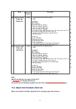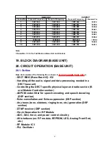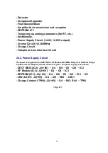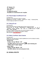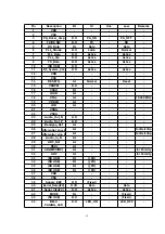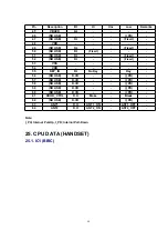
Pin
Description
I/O
Hi
Hi-z
Remarks
89
Power Select
D.O
Low Power
-
-
90
LCD_SEGMENT
D.O
Active
-
-
91
LCD_SEGMENT
D.O
Active
-
-
92
LCD_SEGMENT
D.O
Active
-
-
93
LCD_SEGMENT
D.O
Active
-
-
94
LCD_SEGMENT
D.O
Active
-
-
95
LCD_SEGMENT
D.O
Active
-
-
96
LCD_SEGMENT
D.O
Active
-
-
97
LCD_SEGMENT
D.O
Active
-
-
98
LCD_SEGMENT
D.O
Active
-
-
99
LCD_SEGMENT
D.O
Active
-
-
100
LCD_SEGMENT
D.O
Active
-
-
26. HOW TO REPLACE FLAT PACKAGE IC
26.1. Preparation
- PbF (: Pb free) Solder
- Soldering Iron
Tip Temperature of 700°F ± 20°F (370°C ± 10°C)
Note: We recommend a 30 to 40 Watt soldering iron. An expert
may be able to use a 60 to 80 Watt iron where someone with less
experience could overheat and damage the PCB foil.
- Flux
Recommended Flux: Specific Gravity 0.82.
Type RMA (lower residue, non-cleaning type)
Note: See
ABOUT LEAD FREE SOLDER (PbF: Pb free)
().
26.2. Procedure
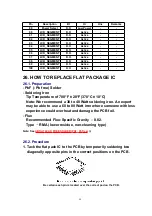
1. Tack the flat pack IC to the PCB by temporarily soldering two
diagonally opposite pins in the correct positions on the PCB.
Be certain each pin is located over the correct pad on the PCB.
58
Summary of Contents for KX-TCD400GC
Page 46: ...18 FREQUENCY TABLE MHz 46 ...
Page 52: ...24 CPU DATA BASE UNIT 24 1 IC2 BBIC 52 ...
Page 56: ...45 MICP A I 56 ...
Page 60: ...60 ...
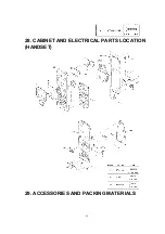
Page 61: ...28 CABINET AND ELECTRICAL PARTS LOCATION HANDSET 29 ACCESSORIES AND PACKING MATERIALS 61 ...
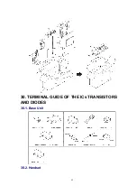
Page 62: ...30 TERMINAL GUIDE OF THE ICs TRANSISTORS AND DIODES 30 1 Base Unit 30 2 Handset 62 ...
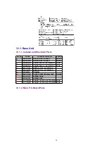
Page 91: ...4 1 5 8 PbF 1 28 18 IC3 IC2 IC1 11 64 1 16 17 32 49 48 33 Marked ...
Page 93: ...Marked PbF IC1 IC2 100 80 5 8 4 1 50 51 30 31 1 11 18 1 28 IC3 ...

